5110: Difference between revisions
Jump to navigation
Jump to search
m (HV Board Pic Added) |
(Added Pictures) |
||
| Line 26: | Line 26: | ||
<gallery> | <gallery> | ||
File:Tek 5110.jpg | File:Tek 5110.jpg | ||
Tek_5110_Front.jpg | 5110 Front Panel | |||
Tek5110Front_2.jpg | 5110 Front Panel | |||
Tek_5110-Back.jpg | Tek 5110 Rear Panel | |||
Tek_5110_Bottom_Coveroff.jpg | 5110 Under Chassis | |||
Tek_5110_LH-Cover-off.jpg | 5110 LH W/O Cover | |||
Tek_5110_Top_Coveroff.jpg | 5110 LH W/O Cover | |||
Tek_5110_A3-Interface.jpg | Tek 5110 A3 Interface Board | |||
Tek_5110_A4-LV-PowerSupply.jpg | Ten 5110 A4 Board | |||
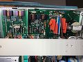
Tek5110_A1_HV-Def.jpg | Tek 5110 A1 - HV Deflection Board | Tek5110_A1_HV-Def.jpg | Tek 5110 A1 - HV Deflection Board | ||
</gallery> | </gallery> | ||
Revision as of 14:37, 6 May 2018

The Tektronix 5110 is a 5000-series three-bay mainframe.
Earlier incarnations of it were known as 5103N and D10. It has a large 8×10 division CRT screen where each division is 0.5 in (12.6 mm) instead of the standard 1 cm per division.
Specifications
It is specified to have a 2 MHz bandwidth with a 5A18N vertical plug-in.
The phase difference between X and Y channels is specified to be less than 1 degree at 100 kHz.
P31 phosphor was standard. P7 and P11 were optional. CRT acceleration voltage is 3,500 V. There is no post-deflection acceleration.
Prices
1990: $2,420
Pictures
-

-
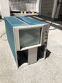
5110 Front Panel
-
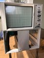
5110 Front Panel
-
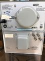
Tek 5110 Rear Panel
-
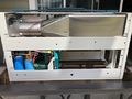
5110 Under Chassis
-
5110 LH W/O Cover
-
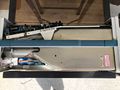
5110 LH W/O Cover
-
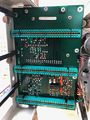
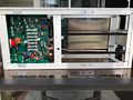
Tek 5110 A3 Interface Board
-
Ten 5110 A4 Board
-
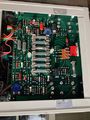
Tek 5110 A1 - HV Deflection Board


