571: Difference between revisions
No edit summary |
No edit summary |
||
| Line 18: | Line 18: | ||
Image:Tek571_params.jpg|571, parameters screen | Image:Tek571_params.jpg|571, parameters screen | ||
Image:Tek571_run_2N2222A.jpg|571, run of a 2N2222A transistor | Image:Tek571_run_2N2222A.jpg|571, run of a 2N2222A transistor | ||
Image:Tek571_10VZener.jpg|571, run of a 1N3020B 10V Zener diode | |||
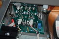
Image:Tek571_innards.jpg|571, inside view | |||
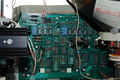
Image:Tek571_socket_pcb.jpg|571, inside view, closeup of socket board | |||
Image:Tek571_relays.jpg|571, inside view, closeup of relays | |||
</gallery> | </gallery> | ||
Revision as of 18:09, 23 April 2013
The 571 is a curve tracer. It can show the characteristic curves of PNP and NPN bipolar transistors, both N- and P-channel FETs, diodes (including Zener types), and SCRs. It is a microprocessor-controlled device, and user interaction is done through navigation keys. A typical sweep run takes about five seconds. It has a parallel printer output that can print graphics on Epson-protocol dot-matrix printers.
One nice feature of the 571 is its ability to store a set of reference curves, which are displayed as a background for subsequent measurement runs. This makes comparison and matching between devices easy.
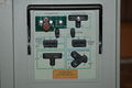
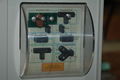
The 571 has a well-designed field of parallel-connected sockets to accommodate many different semiconductor package types. Details can be seen in the photographs below.
Because the nature of electronic component testing involves exposing components to sometimes hazardous voltages and operating conditions, at certain settings the 571 will refuse to start a measurement cycle until the user lowers the built-in hinged plastic shield over the socket area. This is to protect the user from both high voltage and high-velocity flying debris in the event of a catastrophic component failure during a test run. The shield is made of a thick high-impact plastic, and the 571 has an internal microswitch so its firmware knows if the shield is in the up or down position.
-
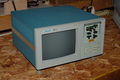
571, front 3/4 view
-
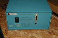
571, rear view
-
571, measurement head, shield up
-
571, measurement head, shield down
-
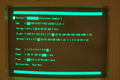
571, parameters screen
-
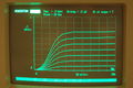
571, run of a 2N2222A transistor
-
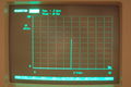
571, run of a 1N3020B 10V Zener diode
-
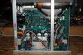
571, inside view
-
571, inside view, closeup of socket board
-
571, inside view, closeup of relays


