7854

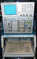
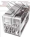
The Tektronix 7854 Waveform Processing Oscilloscope, introduced in 1980, is a 400 MHz combined analog / digital mainframe in the 7000 series that takes two vertical and two horizontal 7000-series plug-ins. In addition to a conventional analog (real time) scope, it contains an equivalent-time sampling 10-bit digitizer and a programmable waveform processor with GPIB interface. Single-shot, pretrigger acquisition is possible with the special 7B87 time base using real-time sampling. The project manager for the 7854 was Tom Rousseau.
The waveform processor can be programmed using a detachable calculator-style keyboard, using postfix operators ("reverse Polish notation" like HP calculators) that operate on entire waveforms, not just individual numbers.
Key Specifications
| Bandwidth | (analog) 400 MHz |
|---|---|
| Fastest cal. sweep | 500 ps |
| Sample rate | 500 kHz (stores repetitive waveforms up to 400 MHz) |
| Resolution | 10 bit |
| Acquisition depth | 128, 256, 512 or 1024 points |
| Memory capacity | 2048 waveform points in up to 16 waveforms (optional expansion to 5120 points and 40 waveforms) |
| Single shot | events and pretrigger up to 50 µs/div ("2.5 µs/point") with the 7B87 Time Base |
| CRT | 154-0644-05 (P-31) or 154-0893-09 (P-11); cathode −3 kV, anode +21 kV, distributed vertical deflection plates |
| Features |
|
Internals
The acquisition system uses what Tektronix termed a "display-oriented random sampling digitizing technique". It simultaneously digitizes a pair of X and Y signal values at a rate of 3.5 µs/point, using Schottky diode bridge based sample/hold circuits and a single 10-bit successive-approximation ADC. The Y sample value is then written into the memory location addressed by the X value, using DMA.
The CPU in the 7854 is a Texas Instruments TMS9900 16-bit microprocessor, known from the infamous TI-99/4 home computer of the late 70s, with 32+6KByte ROM and 8KByte RAM.
The firmware consists of mask ROMs, an FPLA, and patch EPROMs. These ROMs (particularly the early ones from Mostek) are a common point-of-failure. Several remedies exist, outlined here.
Software
Prices
| Year | 1981 | 1990 |
|---|---|---|
| Catalog price | $10,500 | $17,000 |
| 2019 value | $29,360 | $33,060 |
Diagnostic Test Interfaces
- 067-0911-00 Diagnostic Test Interface
- 067-0912-00 Analog Test Card for 7854
- 067-0961-00 Diagnostic Memory Board
Extender Boards
- 067-0913-00 Extender Board 44-Pin (used with the A30-GPIB and A31-ROM Boards)
- 067-0914-00 Extender Board 80-Pin (used with the A27-MPU and A28-RAM Boards)
- 067-0915-00 Extender Board 124-Pin (used with the A26-Control Logic and A29-Display Boards)
Links
- Tek 7854 Design Team
- Tek 7854 @ curiousmarc (with links to videos)
- Tek 7854 @ amplifier.cd
- Tek 7854 @ barrytech.com
- Mostek ROM Repairs @ vintagetek.org
- overview of ROM repair options @ paulcarbone.com
Pictures
-
-

-
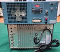
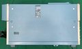
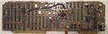
7854 Rear, older version
-
7854 Rear, older version, separate RAM and ROM boards, external battery backup, old-style, silent fan
-
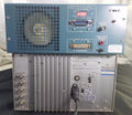
7854 Rear, newer version, combined RAM and ROM boards, internal battery backup, new-style, less silent fan
-
7854 Top
-
7854 Left
-
7854 Right
-
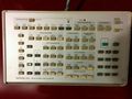
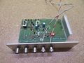
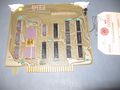
Waveform Calculator Keyboard
-
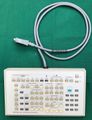
Waveform Calculator Keyboard
-
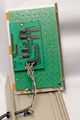
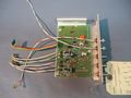
inside the Waveform Calculator Keyboard
-
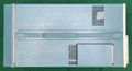
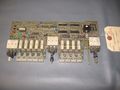
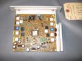
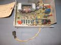
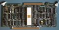
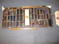
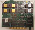
Digital section in the 7854
-
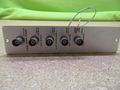
A2 Mode Switch
-
A2 Mode Switch
-

The A7 / Auxiliary regulator
-
A different revision of the A7 board
-
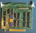
A11 Main Interface
-
A15 Signal Output
-
A15 Signal Output
-
A15 Signal Out Board
-

A17 Horizontal Amp Board
-
A18 Vertical Amp Board
-
A19 Vertical Channel Switch
-
A19 Vertical Channel Switch
-
A20 High Voltage
-
A21 Z-Axis
-
A25 Digitizer
-
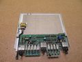
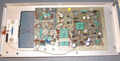
A26 Control Logic Board
-
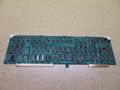
A26 Control Logic Board
-
A26 Control Logic Board
-
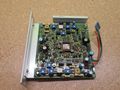
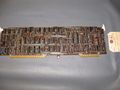
A27 MPU
-
A different revision of the A27 board
-

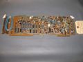
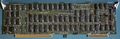
A28 RAM Board
-
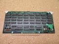
A28 RAM Board with option 2D (RAM Expansion)
-
A29 Display Board
-
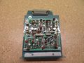
A30 / GPIB board
-
A30 GPIB, different revision
-
A31 ROM Board
-
A32 Rear Panel Connector
-

-

-
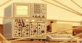
Picture of 7854 during development. Note the different measurement keyboard layout. Picture might date from late 1978
-
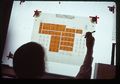
Picture of designing the 7854 waveform calculator keyboard. note the different Keyboard layout.
-
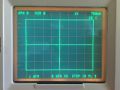
Alignment Pattern
-
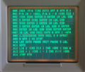
Program for generating Alignment Pattern
-
Mainframe rise time measured with 067-0587-02


Memory Maps
Devices with separated ROM and RAM boards (SN < B100000)
| Address Range | Size | ICs | Purpose | ||
|---|---|---|---|---|---|
| 0000...3FFE | 8k | U100+U110 | ROM | ||
| 4000...7FFE | 8k | U200+U210 | ROM | ||
| 8000...8FFE | 2k | U300+U310 | PATCH ROM “for future use” | ||
| 9000...9FFE | 2k | U400+U410 | PATCH + ROM | ||
| 2k RAM | 4k RAM | 8k RAM | |||
| A000...A7FE | 1k | U510+U520+U530+U540 | x | x | x |
| A800...AFFE | 1k | U610+U620+U630+U640 | x | x | |
| B000...B7FE | 1k | U710+U720+U730+U740 | x | ||
| B800...BFFE | 1k | U810+U820+U830+U840 | x | ||
| C000...C7FE | 1k | U110+U120+U130+U140 | x | ||
| C800...CFFE | 1k | U210+U220+U230+U240 | x | ||
| D000...D7FE | 1k | U310+U320+U330+U340 | x | x | |
| D800...DFFE | 1k | U410+U420+U430+U440 | x | x | x |
| E000...E37E | GPIB, Keyboards, Digitizer,... | ||||
| E380...FFFE | Reserved for Diagnostic Interface | ||||
Devices with combined RAM+ROM Board (SN >= B100000)
| Address Range | Size | ICs | Purpose |
|---|---|---|---|
| 0000...7FFE | 16k | U220+U320 | ROM |
| 8000...9FFE | 4k | U200+U300 | ROM for future use |
| A000...DFFE | 8k | U400+U410 | RAM |
| E000...E37E | 4k | GPIB, Keyboards, Digitizer,... | |
| E380...FFFE | Reserved for Diagnostio Interface |
Devices with installed Diagnostic Boards (all serial numbers)
| Address Range | Size | ICs | Purpose |
|---|---|---|---|
| 0000...0FFE | 2k | U430+U330 | ROM |
| 1000...1FFE | 2k | U410+U310 | ROM |
| 2000...2FFE | 2k | U200+U100 | ROM |
| 3000...3FFE | 2k | U220+U120 | ROM |
| 4000...4FFE | 2k | U420+U320 | ROM |
| 5000...5FFE | 2k | U400+U300 | ROM |
| 6000...6FFE | 2K | U210+U110 | ROM |
| 7000...7FFE | 2K | ROM for future use | |
| 8000...7FFE | 4k | Not used | |
| 9800...9FFE | RAM in Microlab I, disabled when standard ROM is in 7854 | ||
| A000...DFFE | 2...8k | RAM – see tables above | |
| E000...E37E | GPIB, Keyboards, Digitizer,... | ||
| E380...E39E | BKREGCS Breakpoint address register chip select | ||
| E3A0...E3BE | CTREGCS control register chip select | ||
| E3C0...E3DE | BKDATA breakpoint data latch | ||
| E3E0 | F/P Display Data | ||
| E3E2 | F/P Display Data | ||
| E3E4 | F/P Keyboard Data | ||
| E3E6 | F/P Keyboard flag reset | ||
| E3E8 | Terminal I/O Control | ||
| E3EA | Terminal I/O Data | ||
| E3EC | Cassette I/O Control | ||
| E3EE | Cassette I/O Data | ||
| E3F0 | Modem I/O Control | ||
| E3F2 | Modem I/O Data | ||
| E3F4...E3FE | ONBDIO on board input/output to microlab I | ||
| E400...E7FE | RAM in Microlab I | ||
| E800...EFFE | U120+U225 | ROM - bank switched by PROMBK | |
| F000...FFFE | U220+U320 | ROM - bank switched by PROMBK |