Pulse Instruments PI-451: Difference between revisions
Jump to navigation
Jump to search
No edit summary |
No edit summary |
||
| Line 19: | Line 19: | ||
{{Spec | Pulse width | same as input, or ≤100 ns to ≥100 μs, 3 decade ranges + 10:1 variable}} | {{Spec | Pulse width | same as input, or ≤100 ns to ≥100 μs, 3 decade ranges + 10:1 variable}} | ||
{{Spec | Max. frequency | 10 MHz @ 20 V, 20 pF down to 4 MHz @ 25 V, 300 pF }} | {{Spec | Max. frequency | 10 MHz @ 20 V, 20 pF down to 4 MHz @ 25 V, 300 pF }} | ||
{{Spec | Options | | {{Spec | Options | Opt. 002 – digitally programmable output voltage levels (12 bit parallel TTL), plus additional TTL clock input and a high level output on the rear interface | ||
}} | }} | ||
{{EndSpecs}} | {{EndSpecs}} | ||
==Rear interface== | ==Rear interface== | ||
| Line 39: | Line 36: | ||
* 25A – /PS Plugin select, must be 0 to load data | * 25A – /PS Plugin select, must be 0 to load data | ||
* 28A – /MS Mainframe select, must be 0 to load data | * 28A – /MS Mainframe select, must be 0 to load data | ||
'''Data format''' | |||
<code>000000000000</code> = +24.9875 V | |||
<code>011111111110</code> = +0.0122 V | |||
<code>011111111111</code> = 0.0 V | |||
<code>100000000000</code> = −0.0122 V | |||
<code>111111111111</code> = −25.00 V | |||
| | | | ||
* 3B / 4B – mainframe +11.5 V common return = signal ground | * 3B / 4B – mainframe +11.5 V common return = signal ground | ||
| Line 54: | Line 64: | ||
* 24B – Digital input bit 8 | * 24B – Digital input bit 8 | ||
* 25B – Digital input bit 9 | * 25B – Digital input bit 9 | ||
* 26B – DS Data strobe, | * 26B – DS Data strobe, positive edge to load data | ||
* 27B – Digital GND | * 27B – Digital GND | ||
* 28B – LS Level select, 0 = select DAC for low output level, 1 = select DAC for high output level | * 28B – LS Level select, 0 = select DAC for low output level, 1 = select DAC for high output level | ||
|} | |} | ||
</small> | </small> | ||
==Pictures== | |||
<gallery> | |||
Pi-451.jpg | PI-451 | |||
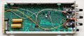
Pi-451 inside.jpg | PI-451 Inside | |||
PI451A front.jpg | PI-451A front | |||
PI451A left.jpg | PI-451A left | |||
PI451A right.jpg | PI-451A right | |||
</gallery> | |||
==Manufacturer== | ==Manufacturer== | ||
| Line 70: | Line 88: | ||
For general-purpose pulse driving on a standalone basis, the modern equivalent is: | For general-purpose pulse driving on a standalone basis, the modern equivalent is: | ||
* [https://www.pulseresearchlab.com/products/prl-470b PRL-470B, Variable Output Pulse Driver, −6 to +10 V, 16 V<sub>p-p</sub>] | * [https://www.pulseresearchlab.com/products/prl-470b PRL-470B, Variable Output Pulse Driver, −6 to +10 V, 16 V<sub>p-p</sub>] | ||
[[Category:Pulse Instruments products]] | [[Category:Pulse Instruments products]] | ||
Revision as of 14:21, 20 February 2022

The Pulse Instruments PI-451 is a MOS/CCD driver plug-in for the TM500 system.
The PI-451 is described as a "MOS/CCD Driver", the PI-451A as a "Programmable Pulse Driver."
A TTL-level input pulse controls an output with programmable high and low voltages and transition times.
Key Specifications
| Output high level | +25 V to –24 V open circuit, or +12.5 V to –12 V into 50 Ω |
|---|---|
| Output low level | +24 V to –25 V open circuit, or +12 V to –12.5 V into 50 Ω |
| Output swing | 1 V min. to 30±3 V max. open circuit, or 0.5 V min. to 15±1.5 V max. into 50 Ω |
| Output level control | manual, voltage programming (1:1, offset ≤80 mV @ ×1 transition time), or (Opt.002) digital |
| Transition time | 2 ns/V to 2 μs/V @ 25 V and 100 pF load, continuously variable in 3 ranges, independent leading and trailing edge controls |
| Trigger input | TTL level, 2−5 V into 50 Ω |
| Trigger output | TTL level, 3 V into 50 Ω, delayed 100 ns from input |
| Delay | 15 ns or ≤100 ns to ≥100 μs from trigger output, 3 decade ranges + 10:1 variable |
| Pulse width | same as input, or ≤100 ns to ≥100 μs, 3 decade ranges + 10:1 variable |
| Max. frequency | 10 MHz @ 20 V, 20 pF down to 4 MHz @ 25 V, 300 pF |
| Options | Opt. 002 – digitally programmable output voltage levels (12 bit parallel TTL), plus additional TTL clock input and a high level output on the rear interface |
Rear interface
Data format
|
|
Pictures
-
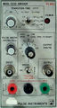
PI-451
-
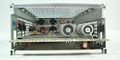
PI-451 Inside
-
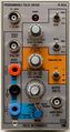
PI-451A front
-
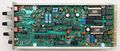
PI-451A left
-
PI-451A right


Manufacturer
For driving FPA and CCD clocks in a multi-channel system, the modern equivalents from Pulse Instruments are:
- PI-41401 Programmable Clock Driver Card, −5 to +8 V, 9 Vp-p
- PI-42460 Programmable Clock Driver Card, ±18 V, 20 Vp-p
For general-purpose pulse driving on a standalone basis, the modern equivalent is: