S-1: Difference between revisions
No edit summary |
No edit summary |
||
| (One intermediate revision by one other user not shown) | |||
| Line 36: | Line 36: | ||
Operating the sampling head without the input connector terminated by a 50 Ω resistor or coaxial | Operating the sampling head without the input connector terminated by a 50 Ω resistor or coaxial | ||
cable will cause a vertical shift of the zero signal baseline by a few millivolts. This is caused by the | cable will cause a vertical shift of the zero signal baseline by a few millivolts. This is caused by the | ||
strobe kickout signal being reflected from the open input connector, and | strobe kickout signal being reflected from the open input connector, and arriving back at the sampling | ||
bridge while the bridge is conducting. | bridge while the bridge is conducting. | ||
</blockquote> | </blockquote> | ||
| Line 54: | Line 54: | ||
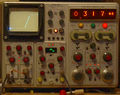
S-52_s-1_rt_brighter.jpg | S-1 in a [[3S2]] sampler / [[567]] scope | S-52_s-1_rt_brighter.jpg | S-1 in a [[3S2]] sampler / [[567]] scope | ||
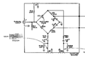
Tek s1 sampler schematic.png|Tektronix S-1 sampler | Tek s1 sampler schematic.png|Tektronix S-1 sampler | ||
Tek 7s11 s-1.jpg|[[7S11]] with S-1 | |||
</gallery> | </gallery> | ||
Revision as of 22:57, 31 August 2019
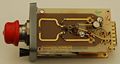
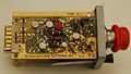
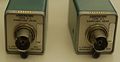
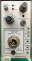
The S-1 sampling plug-in head provides a single GR-874 50 Ω input with a 350 ps rise-time.
The S-1 can be used with the 7000 series of sampling plug-ins, as well as the 3S series of sampling units.
Key Specifications
| Rise time | 350 ps |
|---|---|
| Bandwidth | 1 GHz |
| Input amplitude | −1 V to +1 V with ≤1 Vp-p signals |
| Maximum input | ±5 VDC or sine of 10 Vp-p up to 10 MHz |
| Input impedance | 50 Ω (GR-874) |
| Noise | < 2 mV |
| Features | trigger pickoff for internal triggering |
Links
Internals
The S-1 uses a two-diode sampling gate which has relatively high "kick-out" (leakage of the strobe signal out of the input).
The manual cautions,
Operating the sampling head without the input connector terminated by a 50 Ω resistor or coaxial cable will cause a vertical shift of the zero signal baseline by a few millivolts. This is caused by the strobe kickout signal being reflected from the open input connector, and arriving back at the sampling bridge while the bridge is conducting.
The sampling bridge strobe signal is generated by an avalanche transistor followed by a step recovery diode.
Pictures
-

-
Strobe board
-
Preamp board
-
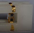
S-1 front
-
Diode mount in S-1
-
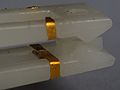
Diode mount in S-1
-
Diode mount in S-1
-
-
Tektronix S-1 sampler
-
7S11 with S-1


