DC501: Difference between revisions
Jump to navigation
Jump to search
Jaredcabot (talk | contribs) (Added service note 050-1276-00) |
Jaredcabot (talk | contribs) (Added Gerber file) |
||
| (One intermediate revision by the same user not shown) | |||
| Line 28: | Line 28: | ||
==Rear Interface == | ==Rear Interface == | ||
{| class="wikitable" | |||
|- | |||
! Connector Pin | |||
! Signal | |||
|- | |||
| 28B || Second decimal point (D2) output | |||
|- | |||
| 27A || Internal scan clock disable input | |||
|- | |||
| 27B || MHz light output | |||
|- | |||
| 26A || Reset input/output | |||
|- | |||
| 25A || TS0 (Time Slot Zero) output | |||
|- | |||
| 25B || External scan clock input | |||
|- | |||
| 24B || Internal scan clock (2 kHz) output | |||
|- | |||
| 23B || Overflow output | |||
|- | |||
| 22B || MSD (most significant digit) | |||
|- | |||
| 20B || 2<sup>8</sup> BCD output, serial by digit | |||
|- | |||
| 20A || 2<sup>4</sup> BCD output, serial by digit | |||
|- | |||
| 21B || 2<sup>2</sup> BCD output, serial by digit | |||
|- | |||
| 19A || 2<sup>1</sup> BCD output, serial by digit | |||
|- | |||
| 19B || Data Good output | |||
|- | |||
| 17A || Signal input ground | |||
|- | |||
| 16A || Signal input | |||
|} | |||
==Gerbers== | |||
* [[Media:670-3300-00.zip|Divide-by-5 circuit board gerbers 670-3300-00]] (ZIP) | |||
==Pictures== | ==Pictures== | ||
Revision as of 04:13, 8 October 2022

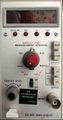
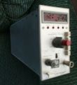
The Tektronix DC501 is a basic 100 MHz frequency counter plug-in for the TM500 system.
Key Specifications
| Input frequency | 10 Hz to 100 MHz |
|---|---|
| Gate time | 10 ms to 10 s in decade steps, plus Manual (totalize count of up to 107 events) |
| Resolution | 7 digits |
| Display | 7-digit LED, overflow indicator |
| Input impedance | 1 MΩ // 20 pF, ×5/×10/×50 attenuator (front) or 50 Ω // 20 pF (rear) |
| Time base stability | ≤1×10⁻⁵; Opt. 1, ≤5×10⁻⁷ (0°C to +50°C after ½h warm-up) |
| Time base drift | ≤1×10⁻⁵; Opt. 1, ≤1×10⁻⁷ (per month) |
Options
- Option 1 – 5 MHz TCXO with 1:5 divider
- Option 2 – Automatic Gate Control and Readout Scaling Circuit (automatically selects the 0 .1-, 1-, or 10-second measurement interval to display the largest number of digits without overflow)
Rear Interface
| Connector Pin | Signal |
|---|---|
| 28B | Second decimal point (D2) output |
| 27A | Internal scan clock disable input |
| 27B | MHz light output |
| 26A | Reset input/output |
| 25A | TS0 (Time Slot Zero) output |
| 25B | External scan clock input |
| 24B | Internal scan clock (2 kHz) output |
| 23B | Overflow output |
| 22B | MSD (most significant digit) |
| 20B | 28 BCD output, serial by digit |
| 20A | 24 BCD output, serial by digit |
| 21B | 22 BCD output, serial by digit |
| 19A | 21 BCD output, serial by digit |
| 19B | Data Good output |
| 17A | Signal input ground |
| 16A | Signal input |
Gerbers
Pictures
-
-
-

Manual photo

