Nicolet 526

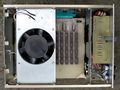
The Nicolet 526 is a signal averager that is used in a modified OEMed Tektronix 5110 (5103N/D10) mainframe. The modifications to the mainframe performed by Nicolet include
- adding a perforated panel for fan cooling via the bottom panel of the scope,
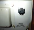
- adding a 12-pin connector on the rear panel of the scope
- connected the 12-pin connector to the interface board, connector J604.
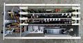
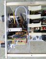
The 526 has its own +5V regulated rail. An LM323 +5V three-terminal regulator is the source of the +5V rail within the Nicolet 526. (Even though the input is marked "+7 UNREG" on the board, it should probably be +7.5V minimum, per the LM323 datasheet.) Since the LM323 is rated for 3 amperes, it is unlikely that the plug-in sinks more than that from the "+7 UNREG" input.
How does the Nicolet 526 get the horizontal signal to the scope if it only plugs into the right vertical plug-in interface connector? In a standard, unmodified 5103, there is no signal path from the right vertical connector to the horizontal amplifier.
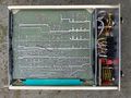
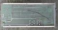
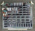
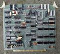
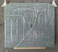
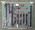
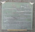
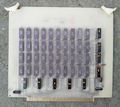
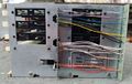
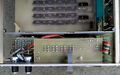
Mechanically, the Nicolet 526 is a three-bay 5000-series plug-in. It mates with the center-bay plug-in connector. The Nicolet 526 is made of four boards and a backplane which has a 40 position two sided edge connector for each board. Connection to the Tektronix mainframe is done via the backplane. The four boards are:
- ADC and Register: The SIGNAL wire from pin 23A on the plug-in interface goes to the inverting input of an LM301 opamp via a resistance of around 165 kΩ. The noninverting input of this opamp is grounded.
- Address
- Control
- Memory
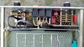
The design makes heavy use of 7400-series digital logic in DIP packages. The printed circuit boards are two-layer. The memory is an array of Fairchild 2102DC MOS 1k x 1 static RAM ICs, DIP, soldered in place.
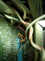
The wires connecting the backplane board on the 526 to the mainframe interface connector on the 526 are labeled:
- H LOCK TRIG (white w/ black stripe), pin 27B of the plug-in connector
- TRIGGER (light violet) 26A
- RO TRIG (violet) 26B
- Y LOCK IN (blue) 25B
- FID SIG (green) maybe "FID" stands for "Free Induction Decay" in NMR? pin 24B on the interface connector, wired to pin 33 of the board #2 (address).
- SIGNAL (brown) 23A
- RO STUS (yellow) 23B
- +7 UNREG (black), pin 22A and 22B of the plug-in connector
- +7 UNREG (black), pin 22A and 22B of the plug-in connector
- GND (white) 14A and 14B (standard 5000-series pinout)
- GND (white) 14A and 14B (standard 5000-series pinout)
- -VERT SIG (white w/ red stripe) 13B (standard 5000-series pinout for vert CH2)
- +VERT SIG (white w/ brown stripe) 13A (standard 5000-series pinout for vert CH2)
- -HORIZ SIG (white w/ orange stripe) 11B
- +30 (red) 5A (standard 5000-series pinout)
- -30 (orange) 5B (standard 5000-series pinout)
- 11A is jumpered to 14B at the male plug-in connector of the 526.
The 12-pin rear-panel connector has its pins numbered on the inside of the connector.
| Pin | Function | Comment |
|---|---|---|
| 1 | ||
| 2 | ||
| 3 | ||
| 4 | ||
| 5 | ||
| 6 | ||
| 7 | ||
| 8 | ||
| 9 | ||
| 10 | +7 UNREG | |
| 11 | ||
| 12 |
-
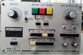
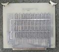
Front
-
Top
-
Left
-
Right
-
Bottom
-
ADC and Register
-
ADC and Register
-
Address Board
-
Address Board
-
Control Board
-
Control Board
-
Memory
-
Memory
-
Rear
-
Top front
-
Right front
-
Bottom front
-

Mainframe rear connector internal
-
Mainframe rear connector external
-
Mainframe rear connector to J604


