M474: Difference between revisions
No edit summary |
No edit summary |
||
| (6 intermediate revisions by 3 users not shown) | |||
| Line 1: | Line 1: | ||
The M474 is the front-end buffer amplifier used in the attenuator modules of the [[11A32]] and [[11A34]]. | {{Monolithic IC | ||
|Manufacturer=Tektronix | |||
|Model=M474 | |||
|Part_nos= | |||
|Description=amplifier | |||
|an=an | |||
|Used_in=11A32;11A34; | |||
|Designers=John Addis;Ivan John Cousins; | |||
}} designed by [[John Addis]]. | |||
The M474 is the front-end buffer amplifier used in the [[119-2000-0x|attenuator modules]] of the [[11A32]] and [[11A34]]. | |||
Regarding the M474, John Addis recalls | Regarding the M474, John Addis recalls | ||
<blockquote> | <blockquote> | ||
I started the design and Ivan “John” Cousins made a very important contribution to it, | I started the design and [[Ivan J. Cousins|Ivan “John” Cousins]] made a very important contribution to it, | ||
namely the addition of Q47 and Q48 and carried it into production. | namely the addition of Q47 and Q48 and carried it into production. | ||
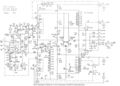
The IC is within the dashed lines. | |||
Outside the dashed lines are two JFETs (probably a matched pair of chips) and a (Tek-made?) fast PNP chip. | The IC is within the dashed lines. Outside the dashed lines are two JFETs (probably a matched pair of chips) and a (Tek-made?) fast PNP chip. | ||
This schematic is of a hybrid, showing the stray inductances. | This schematic is of a hybrid, showing the stray inductances. | ||
The M474's hybrid is separate from but next to the attenuator hybrid inside the attenuator assembly. | |||
The M474 likely tested and trimmed (resistors not shown here) for dc balance before being mounted next to the attenuator hybrid. | The M474 likely tested and trimmed (resistors not shown here) for dc balance before being mounted next to the attenuator hybrid. | ||
R15 is likely trimmed when the M474 is in wafer form. | R15 is likely trimmed when the M474 is in wafer form. R15, R1, R2, and circuitry create the 50 Ω output impedance to match the | ||
R15, R1, R2, and circuitry create the | 11-inch 50 Ω [[Peltola connector|Peltola cable]] from the attenuator to the [[M377]] input. | ||
to match the 11 inch | |||
The attenuator would have been trimmed for input C, attenuation, | The attenuator would have been trimmed for input C, attenuation, | ||
| Line 19: | Line 27: | ||
The M474 contains bootstrap circuitry for the upper JFET so that its operating point does not change with input voltage. | The M474 contains bootstrap circuitry for the upper JFET so that its operating point does not change with input voltage. | ||
(the lower JFET operating point does not change with signal). | (the lower JFET operating point does not change with signal). | ||
This reduces the JFET capacitive loading on the attenuator, makes compensation independent of input signal and, | This reduces the JFET capacitive loading on the attenuator, makes compensation independent of input signal, eliminates thermals and, | ||
more importantly keeps the dc linearity of the whole buffer amplifier good for | more importantly, keeps the dc linearity of the whole buffer amplifier good for | ||
the | the ±2 V of possible input signal given the ±1 V of DV offset applied to the M377 (11A32/11A34 input amplifier). The M377 input is very high impedance so the linearity is very good. | ||
At the time I did not know how to make a Zener diode-like voltage source (that came in the [[M377]]), | At the time I did not know how to make a Zener diode-like voltage source (that came in the [[M377]]), | ||
| Line 30: | Line 38: | ||
<gallery> | <gallery> | ||
11A32,34 attenuator hybrid and M474.jpg|Schematic of M474 and surrounding components | 11A32,34 attenuator hybrid and M474.jpg|Schematic of M474 and surrounding components | ||
Tek 11a32 attenuators.png|M474 and surrounding components designated by "×0.95" and highlighted in red. The 50 Ω resistor to the right of the amplifier symbol is actually inside the M474. | |||
</gallery> | </gallery> | ||
[[Category:Tektronix-made monolithic integrated circuits]] | |||
Latest revision as of 04:57, 15 February 2023
The Tektronix M474 is an amplifier monolithic integrated circuit designed by John Addis. The M474 is the front-end buffer amplifier used in the attenuator modules of the 11A32 and 11A34.
Regarding the M474, John Addis recalls
I started the design and Ivan “John” Cousins made a very important contribution to it, namely the addition of Q47 and Q48 and carried it into production.
The IC is within the dashed lines. Outside the dashed lines are two JFETs (probably a matched pair of chips) and a (Tek-made?) fast PNP chip. This schematic is of a hybrid, showing the stray inductances. The M474's hybrid is separate from but next to the attenuator hybrid inside the attenuator assembly. The M474 likely tested and trimmed (resistors not shown here) for dc balance before being mounted next to the attenuator hybrid. R15 is likely trimmed when the M474 is in wafer form. R15, R1, R2, and circuitry create the 50 Ω output impedance to match the 11-inch 50 Ω Peltola cable from the attenuator to the M377 input.
The attenuator would have been trimmed for input C, attenuation, and capacitive compensation after being mounted and attached to the M474 tested amplifier.
The M474 contains bootstrap circuitry for the upper JFET so that its operating point does not change with input voltage. (the lower JFET operating point does not change with signal). This reduces the JFET capacitive loading on the attenuator, makes compensation independent of input signal, eliminates thermals and, more importantly, keeps the dc linearity of the whole buffer amplifier good for the ±2 V of possible input signal given the ±1 V of DV offset applied to the M377 (11A32/11A34 input amplifier). The M377 input is very high impedance so the linearity is very good.
At the time I did not know how to make a Zener diode-like voltage source (that came in the M377), so there are embarrassing instances of multiple diodes in series.
-
Schematic of M474 and surrounding components
-

M474 and surrounding components designated by "×0.95" and highlighted in red. The 50 Ω resistor to the right of the amplifier symbol is actually inside the M474.

