T7100: Difference between revisions
(cat) |
No edit summary |
||
| Line 6: | Line 6: | ||
amplifier bandwidth. | amplifier bandwidth. | ||
The electron beam | The electron beam passes through terminated helical deflection plates (both X and Y axes use | ||
this form of [[distributed deflection plates]] to achieve the necessary bandwidth), followed by | |||
before it hits the micro-channel plate which consists of parallel channels of 25 μm diameter | an electrostatic scan-expansion lens that increases deflection 4.5 times vertically and 4 times | ||
and offset at a slight angle to the beam. | horizontally, before it hits the micro-channel plate which consists of parallel channels of 25 μm | ||
diameter and offset at a slight angle to the beam. | |||
The inside walls of these channels are coated with resistive material, with a voltage of 700-1050 V applied | The inside walls of these channels are coated with resistive material, with a voltage of 700-1050 V applied | ||
between back and front of the plate. Electrons entering a channel hit the wall where they initiate a cascade | between back and front of the plate. Electrons entering a channel hit the wall where they initiate a cascade | ||
| Line 16: | Line 18: | ||
A final 10 kV potential accelerates the beam across a 3 mm gap toward the phosphor coating. | A final 10 kV potential accelerates the beam across a 3 mm gap toward the phosphor coating. | ||
The beam amplification is sufficient to view a single-shot event at 200 ps/Div with the naked eye. | The beam amplification is sufficient to view a [[Media:Tek7104-200ps-singleshot.jpg|single-shot event at 200 ps/Div]] with the naked eye. | ||
[[File:Micro-channel plate diagram.jpg | 750px |MCP diagram]] | |||
<br />(click image to enlarge) | |||
The Micro Channel Plate's amplification degrades irreversibly with operation, in proportion to the log of total charge passed per channel or display area. For this reason, continued operation with a steady trace and especially at large beam currents must be avoided. To protect the tube, the 7104 contained a protection circuit that shut off the beam after a time depending on the beam circuit. | |||
==Specifications== | ==Specifications== | ||
| Line 28: | Line 33: | ||
==Links== | ==Links== | ||
* [http://www.vintagetek.org/wp-content/uploads/2011/10/7104-Springer-article-email-res.pdf Hans Springer: Breakthroughs throughout push scope to 1 GHz] | * [http://www.vintagetek.org/wp-content/uploads/2011/10/7104-Springer-article-email-res.pdf Hans Springer: Breakthroughs throughout push scope to 1 GHz] | ||
==Screen shots== | |||
<gallery> | |||
File:Tek7104-200ps-singleshot.jpg | 7104 recording a single shot pulse (from [[067-0587-02]]) at 200 ps/Div. Camera: Nikon D7000, 50 mm f/1.4, ISO 3200, 1/2 s. CRT filter not removed. | |||
File:Tek7104-200ps-singleshot-sin1-1g.jpg | 7104 recording 1 GHz sine, single shot at 200 ps/Div. Camera: Nikon D7000, 50 mm f/1.4, ISO 3200, 1/2 s. CRT filter not removed. CRT amplification loss is evident around the center line. | |||
</gallery> | |||
[[Category:Cathode ray tubes]] | [[Category:Cathode ray tubes]] | ||
Revision as of 07:05, 28 October 2015
The Tektronix T7100 (P/N 154-0783-00 with P31 phosphor) is the CRT used in the 7104 and R7103 1 GHz analog scopes. It features a micro-channel plate electron beam amplification stage.
Compared to non-MCP high-speed tubes, the T7100 uses reduced beam current and acceleration voltage to achieve high deflection sensitivity, eliminating the need for high amplifier output voltages, thereby boosting amplifier bandwidth.
The electron beam passes through terminated helical deflection plates (both X and Y axes use this form of distributed deflection plates to achieve the necessary bandwidth), followed by an electrostatic scan-expansion lens that increases deflection 4.5 times vertically and 4 times horizontally, before it hits the micro-channel plate which consists of parallel channels of 25 μm diameter and offset at a slight angle to the beam.
The inside walls of these channels are coated with resistive material, with a voltage of 700-1050 V applied between back and front of the plate. Electrons entering a channel hit the wall where they initiate a cascade of secondary electron emission like in a photomultiplier.
A final 10 kV potential accelerates the beam across a 3 mm gap toward the phosphor coating.
The beam amplification is sufficient to view a single-shot event at 200 ps/Div with the naked eye.

(click image to enlarge)
The Micro Channel Plate's amplification degrades irreversibly with operation, in proportion to the log of total charge passed per channel or display area. For this reason, continued operation with a steady trace and especially at large beam currents must be avoided. To protect the tube, the 7104 contained a protection circuit that shut off the beam after a time depending on the beam circuit.
Specifications
- Screen size: 8 × 10 Div. @ 8.5 mm
- Tube bandwidth: 2.6 GHz
- Resolution: 17 lines / Div.
- Deflection factor: 1 V/cm
Links
Screen shots
-
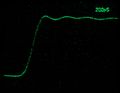
7104 recording a single shot pulse (from 067-0587-02) at 200 ps/Div. Camera: Nikon D7000, 50 mm f/1.4, ISO 3200, 1/2 s. CRT filter not removed.
-
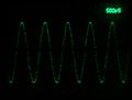
7104 recording 1 GHz sine, single shot at 200 ps/Div. Camera: Nikon D7000, 50 mm f/1.4, ISO 3200, 1/2 s. CRT filter not removed. CRT amplification loss is evident around the center line.

