M753: Difference between revisions
No edit summary |
No edit summary |
||
| Line 1: | Line 1: | ||
The Tektronix M753 is a higher-bandwidth (2 GHz) version of the [[M713]] 1 GHz unity-gain buffer amplifier. | The '''Tektronix M753''' is a higher-bandwidth (2 GHz) version of the [[M713]] 1 GHz unity-gain buffer amplifier. | ||
The M753 is | The M753 is the first amplifier stage in the [[H2462]] input hybrid which is used in several TDS500, TDS600, and TDS700-series scopes. | ||
At the time of the M753's development, [[John Addis]] wrote: | At the time of the M753's development, [[John Addis]] wrote: | ||
| Line 8: | Line 8: | ||
In order to save money, scope input attenuators have been reduced in number over the years to just three | In order to save money, scope input attenuators have been reduced in number over the years to just three | ||
while amplifiers have added either gain switching or internal attenuation to make up for the required missing deflection factors. | while amplifiers have added either gain switching or internal attenuation to make up for the required missing deflection factors. | ||
The three attenuators are usually | The three attenuators are usually ×1, ×10, and ×100. | ||
The | The ×1 attenuator is essentially a straight wire or alternatively just a very small attenuation (typically 10%) | ||
to provide protection to the input JFET. It is very difficult to make a single | to provide protection to the input JFET. It is very difficult to make a single ×100 attenuator, | ||
so the | so the ×100 attenuation is usually a second ×10 attenuator cascaded with the first as needed. | ||
The | The ×1 attenuator is often in cascade with the other attenuator(s) and may be located at the amplifier’s input. | ||
The high frequency response is strictly a function of the path length from the input BNC connector to the JFET input, | The high frequency response is strictly a function of the path length from the input BNC connector to the JFET input, | ||
| Line 27: | Line 27: | ||
There are several advantages inherent in this scheme. | There are several advantages inherent in this scheme. | ||
In this configuration, input from the front panel consists of a | In this configuration, input from the front panel consists of a 50 Ω transmission line | ||
and three different attenuators ( | and three different attenuators (×1, ×10, and ×100) are attached to this line. | ||
A single | A single 50 Ω resistor serves to terminate the line in the 50 Ω (input impedance) mode. | ||
This termination is at the end of the input line instead of at the beginning as with previous attenuators. | This termination is at the end of the input line instead of at the beginning as with previous attenuators. | ||
More commonly now, the | More commonly now, the 50 Ω termination is at the BNC and all the other attenuators are disconnected in 50 Ω input impedance mode. | ||
</blockquote> | </blockquote> | ||
Revision as of 04:39, 15 December 2022
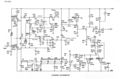
The Tektronix M753 is a higher-bandwidth (2 GHz) version of the M713 1 GHz unity-gain buffer amplifier. The M753 is the first amplifier stage in the H2462 input hybrid which is used in several TDS500, TDS600, and TDS700-series scopes.
At the time of the M753's development, John Addis wrote:
Long ago, high frequency oscilloscopes had one input attenuator for each calibrated deflection factor. The 540 series plugins, Type CA and L, are examples from the 1950s. In order to save money, scope input attenuators have been reduced in number over the years to just three while amplifiers have added either gain switching or internal attenuation to make up for the required missing deflection factors. The three attenuators are usually ×1, ×10, and ×100. The ×1 attenuator is essentially a straight wire or alternatively just a very small attenuation (typically 10%) to provide protection to the input JFET. It is very difficult to make a single ×100 attenuator, so the ×100 attenuation is usually a second ×10 attenuator cascaded with the first as needed. The ×1 attenuator is often in cascade with the other attenuator(s) and may be located at the amplifier’s input.
The high frequency response is strictly a function of the path length from the input BNC connector to the JFET input, and three inches was considered “short”. Various damping resistors are placed in the signal path to reduce ringing, and the attenuator is really a combination quasi-transmission line structure of 75 to 90 ohms impedance at high frequencies and a high impedance RC divider at low frequencies.
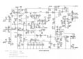
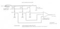
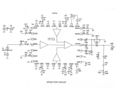
Several years ago, Jim Woo suggested that it should be possible to improve the performance of our input attenuators and reduce their cost if the attenuation selection were done in part by selecting separate amplifiers for each attenuator. Relays select which attenuator is attached to an input line, but only one attenuator at a time is actually connected to the input line. The amplifier and a relay select which attenuator the output signal comes from. This was not practical until integrated JFETs became available. See the "New Attenuator Scheme" figure.
There are several advantages inherent in this scheme. In this configuration, input from the front panel consists of a 50 Ω transmission line and three different attenuators (×1, ×10, and ×100) are attached to this line. A single 50 Ω resistor serves to terminate the line in the 50 Ω (input impedance) mode. This termination is at the end of the input line instead of at the beginning as with previous attenuators. More commonly now, the 50 Ω termination is at the BNC and all the other attenuators are disconnected in 50 Ω input impedance mode.
-
New Attenuator Scheme
-
-
-
-
-

-
-