DC504: Difference between revisions
Jump to navigation
Jump to search
mNo edit summary |
No edit summary |
||
| Line 23: | Line 23: | ||
{{Spec|Accuracy| Adjustable to within 5×10<sup>-9</sup>}} | {{Spec|Accuracy| Adjustable to within 5×10<sup>-9</sup>}} | ||
{{EndSpecs}} | {{EndSpecs}} | ||
An internal "RPM" mode switch stretches gate times sixfold., giving a longest gate time of 1 minute with a display scaled in revolutions per minute. | |||
==Rear Interface== | |||
* 28A − Hold | |||
* 28B − Gate Out, Totalize Start/Stop | |||
* 27B − Decimal point | |||
* 26A − /Reset | |||
* 25A − TS1 (digit select 1, MSD) | |||
* 24A − TS2 (digit select 2) | |||
* 23B − Overflow | |||
* 23A − TS3 (digit select 3) | |||
* 22A − TS4 (digit select 4) | |||
* 21B − BCD out 2 | |||
* 21A − TS5 (digit select 5, LSD) | |||
* 20B − BCD out 8 | |||
* 20A − BCD out 4 | |||
* 19B − Latch Out (Data Good) | |||
* 19A − BCD out 1 | |||
* 16A − Signal input | |||
* 14A − External Clock | |||
==Pictures== | ==Pictures== | ||
===DC504=== | ===DC504 (1975−1983)=== | ||
<gallery> | <gallery> | ||
Tek dc504 front.jpg|DC504 | Tek dc504 front.jpg|DC504 | ||
| Line 36: | Line 57: | ||
DC504-inside-copper-side.jpg|DC504 inside; copper side | DC504-inside-copper-side.jpg|DC504 inside; copper side | ||
</gallery> | </gallery> | ||
===DC504A=== | ===DC504A (1984−1993)=== | ||
<gallery> | <gallery> | ||
Tek dc504a.JPG | DC504A | Tek dc504a.JPG | DC504A | ||
Tek dc504a front.jpg|DC504A | Tek dc504a front.jpg|DC504A | ||
DC504A_Left_Internal.jpg|DC504A | DC504A_Left_Internal.jpg|DC504A left internal | ||
DC504A_Right_Internal.jpg|DC504A | DC504A_Right_Internal.jpg|DC504A right internal | ||
DC504A_3-4_View.jpg|DC504A 3/4 view | DC504A_3-4_View.jpg|DC504A 3/4 view | ||
</gallery> | </gallery> | ||
Revision as of 13:28, 24 April 2023

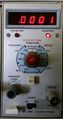
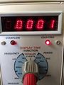
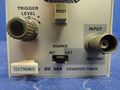
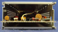
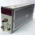
The Tektronix DC504 is a 100 MHz, 5-digit frequency counter plug-in for the TM500 system.
The DC504A successor, introduced in 1984, has 6 digits.
Key Specifications
| Frequency Range | 0 Hz (AC coupled: 10 Hz) to at least 80 MHz |
|---|---|
| Sensitivity (sine wave) | 20 mVRMS below 15 MHz, 35 mVRMS to 50 MHz, derated down to 175 mVRMS at 80 MHz |
| Input impedance | 1 MΩ // 20 pF |
| Trigger Level Range | −1.5 V to +1.5 V |
| Maximum Frequency Resolution | kHz ranges: 0.1 Hz; 1 Hz and 10 Hz (7 digit resolution possible in overflow kHz position); MHz ranges: 100 Hz, 1 kHz (9 digit resolution possible in overflow kHz position) |
| Maximum period resolution | ms ranges: 1 µs, 10 µs; s ranges: 10 ms, 1 ms, 0.1 ms |
| Trigger Error | 0.5% of one cycle at min. trigger sensitivity |
| Display Time | Variable ~0.1 s ... ~10 s and HOLD mode |
| — Internal Standard Time Base (1 MHz) — | |
| Stability | 0°C to +50°C after 30 min warm up: 1×10⁻⁵ |
| Long Term Drift | 1×10⁻⁵ per month |
| Accuracy | Adjustable to within 1×10⁻⁷ |
| — Internal Time Base Option 1 (5 MHz) — | |
| Stability | 0°C to +50°C after 30 min warm up: 1×10⁻⁷ |
| Long Term Drift | 1×10⁻⁷ per month |
| Accuracy | Adjustable to within 5×10⁻⁹ |
An internal "RPM" mode switch stretches gate times sixfold., giving a longest gate time of 1 minute with a display scaled in revolutions per minute.
Rear Interface
- 28A − Hold
- 28B − Gate Out, Totalize Start/Stop
- 27B − Decimal point
- 26A − /Reset
- 25A − TS1 (digit select 1, MSD)
- 24A − TS2 (digit select 2)
- 23B − Overflow
- 23A − TS3 (digit select 3)
- 22A − TS4 (digit select 4)
- 21B − BCD out 2
- 21A − TS5 (digit select 5, LSD)
- 20B − BCD out 8
- 20A − BCD out 4
- 19B − Latch Out (Data Good)
- 19A − BCD out 1
- 16A − Signal input
- 14A − External Clock
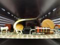
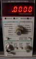
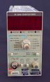
Pictures
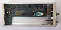
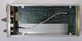
DC504 (1975−1983)
-

DC504
-
DC504
-
DC504
-
DC504
-
DC504
-
DC504
-

DC504 inside; component side
-
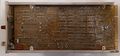
DC504 inside; copper side


DC504A (1984−1993)
-
DC504A
-
DC504A
-
DC504A left internal
-
DC504A right internal
-
DC504A 3/4 view


