FG504: Difference between revisions
No edit summary |
No edit summary |
||
| (26 intermediate revisions by 3 users not shown) | |||
| Line 1: | Line 1: | ||
{{TM500 | mfg=Tektronix | type=FG504 | function=40 MHz function generator | class=function generator | image=Tek | {{TM500 | ||
manuals= | |mfg=Tektronix | ||
* [ | |type=FG504 | ||
|function=40 MHz function generator | |||
|class=function generator | |||
|image=Tek FG504 front 1.jpg | |||
|introduced=1976 | |||
|discontinued=1993 | |||
||manuals= | |||
* [[Media:070-2028-01.pdf|FG504 Instruction Manual (1977)]] | |||
* [[Media:070-2655-00.pdf|FG504 Instruction Manual (SN B0400000+)]] (OCR) | |||
}} | }} | ||
{{BeginSpecs}} | {{BeginSpecs}} | ||
{{Spec | Frequency range | Sine, Triangle and Square | {{Spec | Frequency range | Sine, Triangle and Square – 0.001 Hz to 40 MHz; Ramps, Pulses or asymmetric waveforms – 0.001 Hz to 4 MHz }} | ||
{{Spec | Duty | {{Spec | Duty cycle | 7% to 93% }} | ||
{{Spec | Output | {{Spec | Output amplitude | 30 V<sub>p-p</sub> (OC), 15 V<sub>p-p</sub> (50 Ω) }} | ||
{{Spec | Output | {{Spec | Output attenuator | 0 to 50 dB in 10 dB steps }} | ||
{{Spec | DC | {{Spec | DC offset | ±7.5 V (OC), ±3.75 V (50 Ω) }} | ||
{{Spec | Distortion | ≤ 0.5% from 20 Hz to 40 kHz }} | {{Spec | Distortion | ≤ 0.5% from 20 Hz to 40 kHz }} | ||
{{Spec | Rise/ | {{Spec | Rise/fall time | 6 ns (fixed), 10 ns to 100 ms in 7 steps + variable control }} | ||
{{Spec | Sweep | 1000:1 (500:1 on 10<sup>6</sup> mult.) }} | {{Spec | Sweep | 1000:1 (500:1 on 10<sup>6</sup> mult.) }} | ||
{{Spec | AM input | 10 V<sub>p-p</sub> for 100% }} | {{Spec | AM input | 10 V<sub>p-p</sub> for 100% }} | ||
{{EndSpecs}} | {{EndSpecs}} | ||
==Links== | ==Links== | ||
* [[Media:Tek fg5010 fg507 fg504 description.pdf|Tek FG5010 FG507 FG504 Description]] | |||
* [[Media:Tek fg5010 fg507 fg504 description.pdf|Tek FG5010 FG507 FG504 Description ( | {{Documents|Link=FG504}} | ||
==Rear Interface== | |||
<small> | |||
'''Right (as seen from the front, main board)''' | |||
{| class="wikitable" | |||
|- | |||
! Pin | |||
! Signal | |||
|- | |||
| 28A || Output (via 30 kΩ) | |||
|- | |||
| 27A || Output Common | |||
|} | |||
'''Left (mechanically floating interface board)''' | |||
{| class="wikitable" | |||
|- | |||
! Pin | |||
! Signal | |||
! Pin | |||
! Signal | |||
|- | |||
| 28B || Trig Output Common || 27A || ''nc'' | |||
|- | |||
| 27B || Trig Output || 27A || GND | |||
|- | |||
| 26B || Phase Lock Error Voltage || 26A || Sweep Reset Output | |||
|- | |||
| 25B || Trig/Gate Common || 25A || Linear Sweep Output | |||
|- | |||
| 24B || Trig/Gate Input || 24A || ''nc'' | |||
|- | |||
| colspan="4" | <hr /> | |||
|- | |||
| 23B || ''nc'' || 23A || AM Input | |||
|- | |||
| 22B || VCF Input Common || 22A || Sweep Trigger Input | |||
|- | |||
| 21B || VCF Input || 21A || ''nc'' | |||
|- | |||
|} | |||
</small> | |||
==Internals== | |||
The FG504 takes +/– 33 V from the right slot to create a +/– 15 V supply, and the + 11.5 V for a +5 V supply. | |||
It uses the 25 V<sub>AC</sub> windings, 17.5 V<sub>AC</sub>, and + 11.5 V on the left slot for a +/– 25 V supply to the output amplifier. | |||
The regulators incorporate the mainframe pass transistors on both slots. | |||
U770 is a [[155-0032-00]] below S/N B057720, a [[155-0217-00]] from B057720 on. | |||
==Pictures== | ==Pictures== | ||
'''External''' | |||
<gallery> | |||
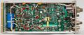
Tek FG504 front 1.jpg | FG504 front panel | |||
Tek fg504 1.jpg | | |||
Tek fg504 2.png | | |||
Tek fg504 3.png | | |||
Tek-fg504-front.jpg | FG504 front panel | |||
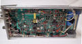
fg504-1.jpg | FG504 in mainframe | |||
Tek fg 504 95.jpg | | |||
Tek fg 504 96.jpg | | |||
Tek fg 504 97.jpg | | |||
Tek fg 504 98.jpg | | |||
Tek fg504 and ps503a.jpg | FG504 and [[PS503A]] in [[TM504]] | |||
Tek fg 504 in tm502a front.jpg | FG504 in [[TM502A]] | |||
Tek fg 504 in tm502a top.jpg | FG504 in [[TM502A]] | |||
</gallery> | |||
'''Internal''' | |||
<gallery> | |||
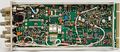
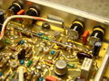
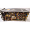
Tek FG504 left.jpg | FG504 left internal | |||
Tek FG504 right.jpg | FG504 right internal | |||
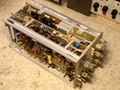
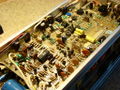
fg504-2.jpg | FG504 without covers | |||
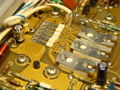
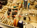
fg504-3.jpg | Main board - output amplifier, attenuator, rise/fall time switch | |||
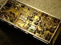
fg504-4.jpg | Detail of output amplifier. Trimmer capacitors for high frequency compensation. | |||
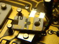
fg504-5.jpg | Detail of 50 Ω attenuator. Divider networks (under the ceramic chips) are switched in or bypassed by cam switches. The 0.3 A output fuse can also be seen. | |||
fg504-6.jpg | Ceramic 10 dB divider lifted to show resistor network. Laser trimming marks can be seen. | |||
fg504-7.jpg | Function generator board that synthesizes the triangle and sine out of a square wave | |||
fg504-8.jpg | Timer board | |||
fg504-9.jpg | Circuit detail | |||
Tek fg504 left internal.jpg | FG504 left internal | |||
Tek fg504 left internal u.jpg | FG504 left internal upside down | |||
Tek fg504 right internal_u.jpg | FG504 right internal upside down | |||
Tek fg504 right internal.jpg | FG504 right internal | |||
Tek fg504 rear.jpg | | |||
Tek fg504 rear2.jpg | | |||
</gallery> | |||
'''Operation''' | |||
<gallery> | |||
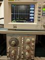
Tek fg504 sine out.jpg | Sine out | |||
Tek fg504 square out.jpg | Square out | |||
Tek fg504 triag out.jpg | Triangle out | |||
</gallery> | |||
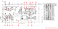
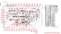
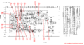
'''Schematics and Locations''' | |||
<gallery> | <gallery> | ||
FG504_A1_Main_Board_Test_Point_Locations.png | A1 Main Board Test Point Locations | |||
FG504_A2_Function_Board_Test_Point_Locations.png | A2 Function Board Test Point Locations | |||
FG504_A3_Loop_Board_Test_Point_Locations.png | FG504 A3 Loop Board Test Point Locations | |||
</gallery> | </gallery> | ||
==Components== | |||
{{Parts|FG504}} | |||
Latest revision as of 12:37, 1 March 2024

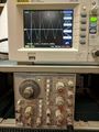
The Tektronix FG504 is a 40 MHz function generator plug-in for the TM500 system.
Key Specifications
| Frequency range | Sine, Triangle and Square – 0.001 Hz to 40 MHz; Ramps, Pulses or asymmetric waveforms – 0.001 Hz to 4 MHz |
|---|---|
| Duty cycle | 7% to 93% |
| Output amplitude | 30 Vp-p (OC), 15 Vp-p (50 Ω) |
| Output attenuator | 0 to 50 dB in 10 dB steps |
| DC offset | ±7.5 V (OC), ±3.75 V (50 Ω) |
| Distortion | ≤ 0.5% from 20 Hz to 40 kHz |
| Rise/fall time | 6 ns (fixed), 10 ns to 100 ms in 7 steps + variable control |
| Sweep | 1000:1 (500:1 on 106 mult.) |
| AM input | 10 Vp-p for 100% |
Links
Documents Referencing FG504
| Document | Class | Title | Authors | Year | Links |
|---|---|---|---|---|---|
| 070-2088-01.pdf | Book | TM500 Series Rear Interface Data Book | 1976 | AF501 • AM501 • AM502 • AM511 • DC501 • DC502 • DC503 • DC504 • DC505 • DC505A • DD501 • DM501 • DM502 • FG501 • FG502 • FG503 • FG504 • LA501 • MR501 • PG501 • PG502 • PG505 • PG506 • PG508 • PS501 • PS502 • PS503 • PS503A • PS505 • RG501 • SC501 • SC502 • SG502 • SG503 • SG504 • SW503 • TG501 • TR501 • TR502 | |
| Tekscope 1976 V8 N1.pdf | Article | New Products | 1976 | FG504 • SG504 • LabCart Model 3 • SW503 • C-5A | |
| Tekscope 1976 V8 N2.pdf | Article | The FG504 - A New Standard in Function Generators | Ira Pollock | 1976 | FG504 |
| Tekscope 1977 V9 N2.pdf | Article | Measuring Harmonic Distortion with a Spectrum Analyzer | Ken Matheson | 1977 | FG504 • 7L5 • 5L4N |
| Tekscope 1978 V10 N2.pdf | Article | Pulse Generator or Function Generator - Making an Intelligent Choice | Bill Rasnake | 1978 | FG504 • PG508 |
Rear Interface
Right (as seen from the front, main board)
| Pin | Signal |
|---|---|
| 28A | Output (via 30 kΩ) |
| 27A | Output Common |
Left (mechanically floating interface board)
| Pin | Signal | Pin | Signal |
|---|---|---|---|
| 28B | Trig Output Common | 27A | nc |
| 27B | Trig Output | 27A | GND |
| 26B | Phase Lock Error Voltage | 26A | Sweep Reset Output |
| 25B | Trig/Gate Common | 25A | Linear Sweep Output |
| 24B | Trig/Gate Input | 24A | nc |
| 23B | nc | 23A | AM Input |
| 22B | VCF Input Common | 22A | Sweep Trigger Input |
| 21B | VCF Input | 21A | nc |
Internals
The FG504 takes +/– 33 V from the right slot to create a +/– 15 V supply, and the + 11.5 V for a +5 V supply. It uses the 25 VAC windings, 17.5 VAC, and + 11.5 V on the left slot for a +/– 25 V supply to the output amplifier. The regulators incorporate the mainframe pass transistors on both slots.
U770 is a 155-0032-00 below S/N B057720, a 155-0217-00 from B057720 on.
Pictures
External


Internal
-
FG504 left internal
-
FG504 right internal
-
FG504 without covers
-
Main board - output amplifier, attenuator, rise/fall time switch
-
Detail of output amplifier. Trimmer capacitors for high frequency compensation.
-
Detail of 50 Ω attenuator. Divider networks (under the ceramic chips) are switched in or bypassed by cam switches. The 0.3 A output fuse can also be seen.
-
Ceramic 10 dB divider lifted to show resistor network. Laser trimming marks can be seen.
-

Function generator board that synthesizes the triangle and sine out of a square wave
-
Timer board
-
Circuit detail
-

FG504 left internal
-
FG504 left internal upside down
-

FG504 right internal upside down
-
FG504 right internal
-

-


Operation
-

Sine out
-
Square out
-
Triangle out


Schematics and Locations
-
A1 Main Board Test Point Locations
-
A2 Function Board Test Point Locations
-
FG504 A3 Loop Board Test Point Locations


Components
Some Parts Used in the FG504
| Part | Part Number(s) | Class | Description | Used in |
|---|---|---|---|---|
| 155-0032-00 | 155-0032-00 • 155-0032-01 | Monolithic integrated circuit | variable-gain transconductance amplifier | 335 • 464 • 465 • 465B • 466 • 475 • 475A • 475M • 634 • 650 • 651 • 652 • 653 • 655 • 656 • 670 • 671 • 7A12 • 475 • FG504 • 1440 • 1460 • 1480 • 1481 • 1482 • 1485 |
| 155-0217-00 | 155-0216-00 • 155-0217-00 | Monolithic integrated circuit | variable-gain transconductance amplifier | 335 • 475 • 7D20 • FG504 |
| CA3046 | 156-0048-00 | Monolithic integrated circuit | transistor array | 7104 • 7403N • 7503 • 7B53A • 7D12 • DM502 • FG504 • S-52 • Telequipment D34 • 7603 • 7613 • 7623 • 7633 |