155-0076-00
The Tektronix 155-0076-00 (M94) is a Tek-made input protection and probe logic integrated circuit in a 16-pin minipac package, designed by John Addis. The M94 has four subcircuits:
- DC current sources for biasing
- Decoder for the probe attenuation pin signal
- RMS detector
- Output logic and drivers for coil of relay that sets input impedance of scope
Biasing
At the bottom of the schematic, there is an NPN current mirror providing 13 current sinks. The mirror is biased such that each of the 13 emitter resistors has one volt across it.
Probe Readout Ring Decoder
The M94 has a circuit for decoding the probe attenuation factor based on the probe readout pin. The probe readout pin contacts the readout ring on the probe input of the scope. The readout ring is pulled up to 5 volts by a 5 kΩ resistor outside of the M94. Inside the probe, there is a resistor between the readout pin and the ground of the BNC connector. This scheme allows the scope to distinguish 1x, 10x, and 100x probes, and adjust on-screen readout scale accordingly, so that the on-screen scale is referenced to the voltage at the probe tip. Letting the ring float represents a 1x probe. 11 kΩ to ground represents a 10x probe. 6.2 kΩ to ground represents a 100k probe.
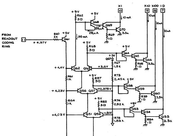
When the ring is left floating, it is pulled up to 5 volts. In this case, the voltages are as shown in the schematic. Q62, Q56, and Q51 are on, and Q63, Q57, and Q52 are off. Current is allowed to flow out of the base of Q68, and consequently the darlington pair of Q69 and Q70 is turned on, sinking current from the X1 pin of the M94.
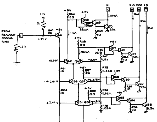
When a 10x probe is connected, the voltage of the probe pin ring is determined by a voltage divider formed by the 5 kΩ resistor (to +5 V) in the scope and the 11 kΩ resistor (to ground) in the probe. The voltage at pin 11 of the M94 is 3.44 V. Q62 is off and Q63 is on. Current is allowed to flow out of the base of Q64, and Q65 and Q66 are on. The X10 pin of the M94 is sinking current.
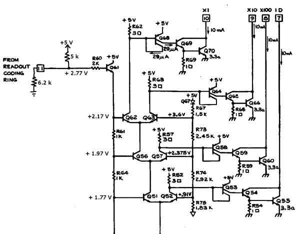
When a 100x probe is connected, the voltage at pin 11 is 2.77 V. Q57 is on and Q56 is off. Since Q56 is off, there is no tail current in the Q62/Q63 pair. The collector of Q57 pulls current from the base of Q58, which turns on Q59 and Q60. The X100 pin sinks current.
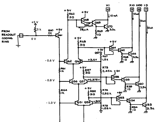
Some probes have an "identify" button. When pressed, that button shorts the probe detect pin to ground. In that situation, pin 11 of the M94 is at ground potential and the identify switch is sinking 200 μA from the 5 kΩ pullup resistor. Q52 is on. Q51 is off, and there is no tail current in Q56/Q57, and the same with Q62/Q63. The ID pin is sinking current.
RMS Converter
Output Logic
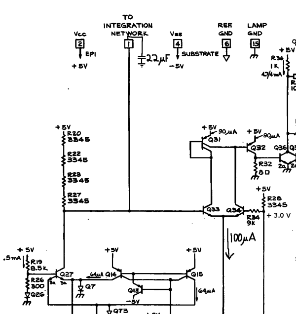
The objective of the output logic is to protect the 50 Ω input attenuator from overheating. The strategy is to build an electrical model of the 50 Ω attenuator's thermal dynamics, and to disconnect the input signal from the relatively fragile 50 Ω attenuator if further electrical input would put it at risk of overheating.
The collector current of Q27 is quasi-proportional to the instantaneous power dissipated in the 50 Ω input attenuator. This current is applied to a leaky integrator. The electrical time constant of the leaky integrator matches the thermal time constant of the most vulnerable parts of the 50 Ω input attenuator. In the case of the 11A52, this is a simple RC circuit with a time constant of 294 milliseconds. The voltage at pin 1 (base of Q33) is inversely related to the modeled temperature of the attenuator.
A 3.0 volt reference is established at the base of Q34.
The voltage on pin 1 is compared with the 3.0 volt reference.
When the input is not overloaded, the 0.1 mA tail current of Q33/Q34 is steered to the Q33's side and Q32 is cut off.
When the input is overloaded, the voltage at the base of Q33 dips below 3.0 volts, and the the tail current is steered to Q34's side.
This turns on Q32.
Thus, the collector current of Q32 is essentially a digital signal: on means overload, off means no overload.
Q36, Q37, Q38, and Q39 form an RS flip-flop. When input overload is detected, Q32 turns on, supplying current to the base of Q36. The collector voltage of Q36 and Q37 goes to around 0 V. The pin 13 "MODE INPUT" pin is normally grounded (e.g., in the 485. In this state, Q38 and Q39 are cut off and their collectors are pulled up by R38. That causes a current to flow through R53, into the base of Q37, which keeps the collectors of Q36 and Q37 close to ground potential. So, once an overload condition is detected, the flip flop stays in the left-side-active state even after the input is removed.
When the excessive input signal has been removed and the operator wants to re-enable the 50 Ω input, pin 13 of the M94 is momentarily allowed to float high. In the 485, this is done by the operator pressing the impedance selector button on the front panel, S125B. Letting pin 13 float allows current to flow through R45, into the base of Q39. The resulting collector current in Q39 pulls the collector of Q38/Q39 low, which stops the current in R53, thus turning off Q37. Q36 is also off because the excessive input has been removed. So the collector of Q36/Q37 is pulled high by R36, which also turns on R38. This leaves the flip-flop in the stable right-side-active state.
Used in
Datasheet
Links
-
M94 as U80 in 485
