DF2: Difference between revisions
No edit summary |
No edit summary |
||
| Line 39: | Line 39: | ||
The DF1 is built around a [[Motorola 6800]] microprocessor with three 2K×8 masked ROMs (one on a ROM expansion board) and sixteen 1K×1 SRAMs (2101). | The DF1 is built around a [[Motorola 6800]] microprocessor with three 2K×8 masked ROMs (one on a ROM expansion board) and sixteen 1K×1 SRAMs (2101). | ||
The 7D01 | The DF2 and 7D01 are often affected by [[bad TI IC sockets]], see [[7D01/Repairs|the Repairs tab]]. | ||
==Pictures== | ==Pictures== | ||
Revision as of 12:49, 16 January 2022
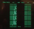
The Tektronix DF2 is a display formatter for use with the 7D01 logic analyzer. It is a DF1 with special support for debugging GPIB, from which it differs by having an extra front-panel "MENU" key and a daughter board with additional ROMs.
The DF2 does not, however, have a GPIB interface of its own − it can only analyze external GPIB traffic. This functionality is invoked with the added MENU control (refer to the instruction manual for details).
Project manager for the DF2 was Murlan Kaufman.
A 103-0209-00 GPIB to probe comb adapter was supplied with the DF2. This connects GPIB DIO1..DIO8 to CH8..CH15, DAV to the CLOCK input, ATN to CH7, EOI to CH6, SRQ to CH5, and REN to CH4. GPIB signals DAV, NRFD, NDAC and IFC brought out to pins on the connector. CH3..0 are user defined inputs that can track any of these signals, or others as needed. For GPIB analysis, bus data is acquired synchronously using the negative-going edge of the GPIB DAV (Data Valid) line as an external clock.
Key Specifications
| Memory | One reference table memory, same as 7D01 capacity (max. 16 channels at 254 bits/ch) |
|---|---|
| Display modes |
|
| Reset output | Positive 100 μs pulse, ≤0.4 V / ≥2.4 V |
Internals
The DF1 is built around a Motorola 6800 microprocessor with three 2K×8 masked ROMs (one on a ROM expansion board) and sixteen 1K×1 SRAMs (2101).
The DF2 and 7D01 are often affected by bad TI IC sockets, see the Repairs tab.
Pictures
Custom ICs used in the DF2
No results


