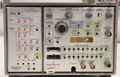
DF1

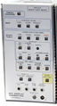
The Tektronix DF1, introduced in 1977, is a "display formatter" for use with the 7D01 logic analyzer. It adds "data domain displays" (binary, octal and hexadecimal state tables, and a function map display) to the 7D01's time-domain display. It can store a reference table, to which the captured data can be compared. The DF1 was introduced in 1977.
The Tektronix DF2, introduced in 1978, is the same as the DF1 with the exception of an added front-panel "Menu" key and an additional ROM (on a daughter board) that supports GPIB and ASCII modes.
The DF2 does not have a GPIB interface, it can only analyze external GPIB traffic. For this purpose, a 103-0209-00 GPIB to probe comb adapter was supplied with the DF2, which connects GPIB DIO1..DIO8 to CH8..CH15, DAV to the CLOCK input, ATN to CH7, EOI to CH6, SRQ to CH5, and REN to CH4. GPIB signals DAV, NRFD, NDAC and IFC brought out to pins on the connector. CH3..0 are user defined inputs that can track any of these signals, or others as needed. For GPIB analysis, bus data is acquired synchronously using the negative-going edge of the GPIB DAV (Data Valid) line as an external clock.
From TekScope V.8 N.4 1976:
Project manager for the DF1/DF2 was Murlan Kaufman, with Dave Lowry and Jeff Bradford doing the electrical and software design, and Ed Wolfe doing mechanical design. Roy Kaufman and Joe Gaudio, Evaluation Engineers, and Dave McCullough, Marketing Program Manager, also made valuable contributions. Special thanks are due to Jack Lyngdal and Nick Colvin, Manufacturing; Betty Spohn, ECB; Jan Bowden, Prototypes; and to everyone else who contributed to a a speedy, efficient completion of the project.
Key Specifications
| Memory | One reference table memory, 1KB, same as 7D01 capacity (max. 16 channels at 254 bits/ch), plus 1KB display RAM |
|---|---|
| Display modes |
7D01/DF1 or DF2
7D01/DF2
|
| Reset output | Positive 100 μs pulse, ≤0.4 V / ≥2.4 V |
Links
Documents Referencing DF1
| Document | Class | Title | Authors | Year | Links |
|---|---|---|---|---|---|
| Tekscope 1976 V8 N4 with Supplement.pdf | Article | A Display Formatter – The Indispensable Tool for the Data Domain | Dave Lowry • Jeff Bradford | 1976 | DF1 • 7D01 |
| AX-3524.pdf | Application Note | Troubleshooting a Microprocessor (Logic Analyzer App Note #57K1.0) | 1977 | 7D01 • DF1 |
Documents Referencing DF2
| Document | Class | Title | Authors | Year | Links |
|---|---|---|---|---|---|
| Tekscope 1978 V10 N1.pdf | Article | New Products | 1978 | DF2 • P6303 • C-28 • 8001 • CT8100 • 4014-1 | |
| Tekscope 1978 V10 N2.pdf | Article | Unraveling the Mystery on the GPIB | Bruce Ableidinger | 1978 | DF2 • 7D01 • P6451 • GPIB |
Internals
An internal jumper allows the user to select the source of the on-screen readout in timing diagram mode, which can be either the mainframe readout supplied by the 7D01, or superimposed by the DF1/DF2. The latter is the standard setting and allows the DF1/DF2+7D01 combination to be used in mainframes without readout, e.g. the large-screen 7603N.
The DF1/DF2 has no direct connection to the scope mainframe − it attaches to the 7D01 through a 50-pin D-sub connector on the right side panel only. The DF1/DF2 and 7D01 are mechanically coupled by three nylon standoffs that slide into cutouts in the 7D01's case rails. The bottom two standoffs are fixed and are inserted first, then the connector is plugged in and the third, sliding, stand-off at the top is moved to its locked position.
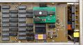
The DF1/DF2 is built around a Motorola 6800 microprocessor with two (DF2: three) 2K×8 masked ROMs and sixteen 1K×1 SRAMs (Intel 2102).
The DF1, DF2 and 7D01 are often affected by bad TI IC sockets and/or ROM failures, see the Repairs tab.
Memory map
| Address (hex) | Use |
|---|---|
| 0000-007F | Scratchpad RAM (U274, Motorola 6810A) |
| 0080-00FF | I/O registers |
| 4000-47FF | ROM U820 on DF2 expansion board (156-1132-00, 2k×8, 6831B) |
| 4800-4FFF | ROM socket on DF2 expansion board, unused |
| 5000-57FF | ROM socket on DF2 expansion board, unused |
| 5800-5FFF | ROM socket on DF2 expansion board, unused |
| 6000-63FF | 1KB RAM |
| 8000-63FF | 1KB display RAM, "write-only" |
| Axxx | Vertical map address register (→ U552, U554) |
| Cxxx | Horizontal map address register (→ U452, U454) |
| F000-F7FF | ROM U294 (156-0900-00, 2k×8, GI RO-3-8316 or Mostek MK31000) |
| F800-FFFF | ROM U284 (156-0899-00, 2k×8, GI RO-3-8316 or Mostek MK31000) |
Pictures
DF1
-
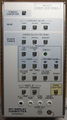
DF1 front panel
-
-
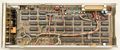
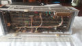
DF1 internal, right side
-
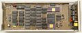
DF1 internal, left side, ROM chips removed from sockets
-

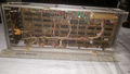
DF1 internal, left side, with ROM replacement piggyback board (prototype)
-
ROM replacement piggyback board (production)
-

DF1 front with faceplate removed, showing keyboard PCB. Note three unpopulated key positions.
-

-

Side connector
-
-
-


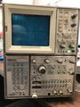
DF2
-
DF2 front panel
-
-
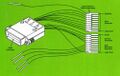
103-0209-00 GPIB probe


Displays
-
Timing diagram with mainframe readout
-
Timing diagram with DF readout
-
Timing diagram zoomed
-

Map diagram with octal cursor-position readout
-
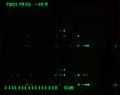
Map diagram with binary cursor-position readout
-

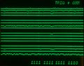
Octal state table without reference
-
Binary state table with reference
-
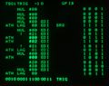
DF2 GPIB table (random data)
-

DF2 ASCII table (16 bit mode in 2 columns). Note lowercase character "o" is displayed as <O>.
-
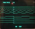
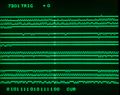
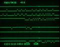
7D01 + DF1/DF2 Timing Diagram (with DF1/DF2 readout)
-
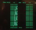
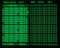
7D01 + DF1/DF2 State Table example - 8 bit mode, 7D01 table left with highlighted differences to DF1/DF2 reference table on the right


Components
Some Parts Used in the DF1
Some Parts Used in the DF2
| Part | Part Number(s) | Class | Description | Used in |
|---|---|---|---|---|
| Intel 2102 | 156-0291-00 | Monolithic integrated circuit | 1K×1 static RAM | 833 • DF1 • DF2 • P7001 • Nicolet 526 |
| Mostek MK31000 | Monolithic integrated circuit | 2k×8 mask-programmable ROM | DF1 • DF2 | |
| Motorola 6800 | 156-0426-00 • 156-2413-00 • 156-5472-01 | Monolithic integrated circuit | 8-bit microprocessor | 021-0206-00 • 021-0374-00 • 067-0902-00 • 067-1137-99 • 222 • 222A • 222PS • 2424L • 2445 • 2465 • 2467 • 4051 • 7250 • 7912 • 7912AD • 7A16P • 7A29P • 7B81P • 7B90P • 833 • 834 • 835 • 836 • CG5001 • CG551AP • CG5010 • CG5011 • DF1 • DF2 • DM5010 • FG5010 • MI5010 • SI5010 • PS5004 • PS5010 • SG5010 • Keithley 181 • Keithley 182 • Keithley 175 • Keithley 175A • Keithley 191 • Keithley 192 • Keithley 195 • Keithley 195A • Keithley 197 • Keithley 220 • Keithley 224 • Keithley 230 • Keithley 263 • Keithley 485 • Keithley 580 • Keithley 617 |
| Motorola 6810 | 156-0716-00 | Monolithic integrated circuit | 128×8 static RAM | 021-0206-00 • DF1 • DF2 • Keithley 181 |