11401
The Tektronix 11401 is a 500 MHz digitizing scope with three plugin bays accepting 11000-series plugins and 7000-series plug-ins. The 11401 and 11402 (which has 1 GHz bandwidth) differ only in their sampler board. In all other respects, the 11401 and 11402 are the same.
Project manager of the 11400 series was Tom Rousseau, who was also project manager for the 7854. The 11400 engineering team included some of the main people from the 7854 project.
The 11401 mainframe uses equivalent time sampling at a rate of 20 MHz (20 Msps). Each sample has 10 bits of resolution. It is capable of displaying eight separate 10 bit resolution traces at one time. The mainframe is fully remotely programmable over RS-232 or GPIB.
This mainframe accepts up to three plugins with differing numbers of channels and bandwidths. For example, each 11A52 plugin allows two inputs at 500 MHz bandwidth (50 Ω only input impedance). The 11A34 plugin allows four inputs at 300 MHz bandwidth, and the 11A32 allows two channels at 300 MHz. Three 11A34 plugins then allow up to 12 channels of information, but the mainframe limits the number displayed at any one time to eight. The other four channels may still be used for triggering. The 11402 and (later) 11403 and DSA600 mainframes allow up to 1 GHz of bandwidth with an 11A71 with one 50 Ω input, or two 50 Ω inputs in the (later) 11A72.
Key Specifications
- please add
Resolution is up to 10 ps horizontal and 10 bits vertical, with 10,240 points of memory.
Internals
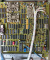
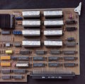
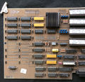
Note: The photos of the "Prototype 11401" are of a scope that said 11331 on the front panel.
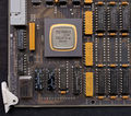
The 11401 uses the 156-2622-00 SDI controller IC (U330).
Vertical Signal Path
Each of the three plug-in bays in the 11401 has a dedicated sampler. The sampling clock is common to the three samplers.
The sampling pulse is generated by an ECL 2-input OR gate being fed SAMPLE_CLOCK and delay_5ns(invert(SAMPLE_CLOCK)). This produces 5 ns pulses with rise time around 1 ns, which are fed to a discrete NPN differential pair operating in a clipping current-switch mode, resulting in faster edges. The output of the differential pair drive a strobe generator IC, U1040, which is an M453 die, packaged as part number 155-0320-00 or 155-0320-01, depending on the mainframe's serial number. U1040 has three sampling strobe outputs, which are fed to the sampling gates.
The plug-in connector's differential "DISPLAY" pins are connected to the samplers by coaxial cable, i.e. there are no high-speed amplifiers in the mainframe's signal path. The DISPLAY+ and DISPLAY- signals are fed to separate samplers. The sampled signals are combined in the channel switch to obtain a single-ended signal that is fed to the ADC.
The outputs of the sampling gates are multiplexed by a channel switch into an ADC. A two-stage pipelined ADC (Tek part number 155-0289-01) is used, with five bits per stage. Each stage has a bank of 32 comparators.
The output of the ADC is stored in RAM. The contents of the RAM may have many points depending on the size of the acquisition window. The "Waveform Compressor" board takes the contents of the acquisition RAM and renders it to 512 points on the horizontal axis for display.
Links
Pictures
-
-
-
Prototype 11401 LV PSU diagnostic LEDs
-
Prototype 11401 LV PSU Control Rectifier
-
Prototype 11401 LV PSU Inverter
-
Prototype 11401 TImebase Board
-
Prototype 11401 Trigger 155-0239-02
-
Prototype 11401 acquisition board right
-
Prototype 11401 acquisition board left
-
Prototype 11401 acquisition board
-
Prototype 11401 bottom internal
-
Prototype 11401 bus signals
-
Prototype 11401 waveform compressor back
-
Prototype 11401 waveform compressor front
-
Prototype 11401 670-8858 board back
-
Prototype 11401 670-8858 board front
-
Prototype 11401 I/O board back
-
Prototype 11401 I/O board front
-
Prototype 11401 display side
-
Prototype 11401 display top
-
Prototype 11401 bus socket
-
Prototype 11401 bus
-
Prototype 11401 670-8855 board rear
-
Prototype 11401 670-8855 board front
-
Prototype 11401 1562472-00
-
Prototype 11401 memory board rear
-
Prototype 11401 memory board front right
-
Prototype 11401 memory board front left
-
Prototype 11401 memory board front
-
Prototype 11401 display controller right
-
Prototype 11401 display controller left
-
Prototype 11401 display controller
-
Prototype 11401 top internal
-
11401 right side
-
11401 rear


