P6230
The Tektronix P6230 and P6231 are passive ×10 (450:50 Ω) probes with 1.5 GHz bandwidth and DC offset capability, intended to minimize DC probe-loading effect when used on logic circuits.


The P6230 has an offset control potentiometer in the termination box and connects to the scope, e.g. 7000 series scopes, through a BNC connector with ×10 readout pin. It can be powered from 7000 series mainframes having LEMO S-series connectors for probe power, or compatible units such as the 1101. The 7A42 can measure the P6230's offset.
The P6231 is a TekProbe Level 2 probe intended for 11000 series plugins such as the 11A32 or 11A71. Offset control and power are provided by the scope mainframe through a Tekprobe BNC connector.
The P6230/6231 shares accessories with many other Tektronix subminiature modular probes although the input hybrid is unique. Tip color is yellow, connector end color is blue, part number 206-0279-00. Its end to end resistance is 400 Ω.
Key Specifications
| Bandwidth | DC to ≥ 1.5 GHz |
|---|---|
| Rise time | ≤ 230 ps |
| Attenuation | 10× |
| Input Impedance | 450 Ω // 1.3 pF (1.6 pF guaranteed) |
| Signal delay | 8.7 ± 0.1 ns |
| DC offset | −5 V ≤ (Vsignal + Voffset) ≤ +5 V |
| Features |
|
Internals
The P6230/6231 probes are sometimes described as FET probes or active probes, however, as the circuit diagram clearly shows, this is not correct. After the 400 Ω input hybrid, the AC component of the input signal is connected directly to the scope input through a 1 μF capacitor, then terminated in 50 Ω either in the scope input or the switchable terminator. The active circuit in the P623x, a standard NE5532 dual opamp, has the function of restoring and offsetting the input signal's low-frequency and DC components. This approach is similar to the feed-beside technique used in the 7104 scope and 7A29 amplifier.
Tek explains the raison d'être for the P6230/P6231 thus:
The P6230 acts as a standard 500 Ω passive voltage probe with the additional capability of having an adjustable tip "nulling voltage." This feature reduces the dc-loading effects on the probe when it is used to measure signals whose mid-voltage value is other than zero volts, or in circuits where the termination impedance is returned to other than ground level. The Input Bias/Offset Voltage may be adjusted so that at a particular test-signal voltage both ends of the probe input-resistor are at equal potentials and no current is flowing through the resistor.
ECL logic is most commonly operated from a −5.2 V supply with VCC connected to ground. The output of an ECL gate is the emitter of an NPN emitter follower stage. The output is pulled down to a negative supply (about −2 V) with an external resistor (50 Ω to 100 Ω). Since speed is a major consideration in ECL designs, the interconnections between gates are often transmission lines, and the pull-down resistor doubles as a line termination.
If a standard 500 Ω, 10× probe without the input Bias/Offset feature were used to examine an ECL output, the probe's 500 Ω resistance to ground would form a voltage divider with the gate's output-termination resistor. This divider can cause distortion of the output signal levels, shift the DC operation point of the output transistor, and reduce the gate's noise margin.
The DC-load nulling capability of the P6230 helps to solve this problem. By adjusting the Input Bias/Offset Voltage to the ECL low level or to the termination voltage, the only effect of the probe resistance will be a small decrease in the ECL output-termination resistance. The effect of the probe on output voltage levels is negligible.
Links
Prices
| Year | 1984 | 1987 | 1989 | 1991 | 1995 |
|---|---|---|---|---|---|
| P6230 Catalog price | $385 | $395 | $420 | $525 | – |
| In 2023 Dollars | $1,100 | $1,100 | $1,000 | $1,200 | – |
| P6231 Catalog price | – | $410 | $410 | $525 | $799 |
| In 2023 Dollars | – | $1,200 | $1,000 | $1,200 | $1,600 |
Pictures
-
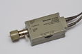
P6230 compensation box
-
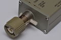
P6230 Switchable terminator
-
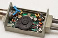
P6230 Compensation box interior
-
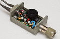
P6230 Compensation box interior
-
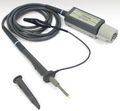
P6231
-
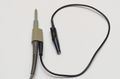
P6230 probe tip with alligator clip ground lead
-
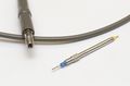
-
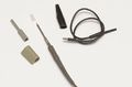
Probe tip components
-
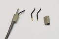
Low-inductance ground lead
-

-
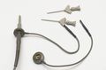
-
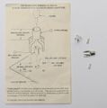
Probe-to-PCB adapters
-
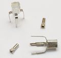
Probe-to-PCB adapters
-
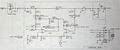
P6230 circuit diagram
-
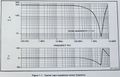
P6230 input impedance graph


Measurements
-
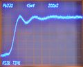
-
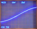
P6230 Rise time without ground lead: 9.2 * 20 ps = 184 ps (equiv. to 1.9 GHz bandwidth)
-
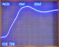
Effect of using the "low inductance" ground lead - rise time 400 ps, bandwidth 875 MHz
-
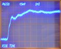
Using the 250 mm (9.8") alligator ground lead - severe pulse distortion, rise time ~3 ns (115 MHz)!
-
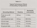
Bandwidth vs. grounding, from manual


