7104: Difference between revisions
| Line 51: | Line 51: | ||
The 7104 uses a switch-mode power supply. | The 7104 uses a switch-mode power supply. | ||
Module A23 (schematic page <14>) contains the mains rectifier, base drive circuitry, and power transistors of the inverter (aka, switcher). | Module A23 (schematic page <14>) contains the mains rectifier, | ||
These transistors produce a 25 kHz waveform that is fed to the primary of T1310, whose secondaries provide the power for the rest of the scope. | base drive circuitry, and power transistors of the inverter (aka, switcher). | ||
These transistors produce a 25 kHz waveform that is fed to the primary of T1310, | |||
whose secondaries provide the power for the rest of the scope. | |||
Module A24 (also on schematic page <14>) contains the inverter control circuit and rectifiers for the secondaries of T1310. | Module A24 (also on schematic page <14>) contains the inverter control circuit | ||
and rectifiers for the secondaries of T1310. | |||
The inverter control circuit uses the [[155-0067-02]] inverter control IC, which is U1275. | The inverter control circuit uses the [[155-0067-02]] inverter control IC, which is U1275. | ||
Module A25 (schematic page <15>) contains the low-voltage regulators. | |||
There as independently regulated and current-limited sections | |||
for the -50V, -15V, +5V, +15V and +50V rails. | |||
Each section has an opamp and a BJT output transistor in emitter-follower configuration. | |||
The opamps need power, too. | |||
To avoid a dependency cycle, the power supplies for the opamps are separate | |||
low-current, low-efficiency zener clamps that in no way depend on the -50V, -15V, +5V, +15V or +50V regulators. | |||
The power supplies for the opamps produce -22V, -5.6V, +5.6V, and +22V. | |||
To avoid exceeding the opamps' limit of 30V total rail voltage, each opamp either gets | |||
-22V and +5.6V, or -5.6V and +22V, depending on whether it needs more output swing | |||
in the positive or negative direction. | |||
The +50V section is produces the reference voltage for the other sections. | |||
It uses a 9V zener diode, VR1412, as a reference. | |||
==Prices== | ==Prices== | ||
Revision as of 12:09, 8 April 2018
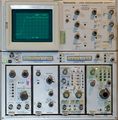
The Tektronix 7104 is a 1 GHz, non-storage 7000-series oscilloscope mainframe that takes two 7000-series vertical plug-ins and two 7000-series horizontal plug-ins. It was introduced in 1978. There is also a rack-mount version, the R7103, albeit with only one horizontal bay.
The scope employs a micro-channel plate (MCP) CRT design to get good screen intensity at high sweep speeds with moderate acceleration voltage.
The high speed necessitated using distributed deflection plates also for the horizontal deflection system, which reaches a bandwidth of 350 MHz. Option 2 adds a horizontal delay line to make the high horizontal bandwidth available for X-Y mode at a phase shift of <2° up to 50 MHz, nullable at any frequency up to 250 MHz.
The 7A29 1 GHz vertical amplifier and the 7B15/7B10 time base pair were introduced along with the 7104 to match the system bandwidth.
Key Specifications
| Bandwidth | 1 GHz (with 7A29) – rise time < 350 ps |
|---|---|
| Fastest calibrated sweep | 200 ps/Div (with 7B10) |
| Calibrator | 40 mV to 4 V (p-p) in decade steps, 1 kHz; 4 mV to 400 mV into 50 Ω; 40 mA with adapter |
| Y delay line | 51 ns (frequency compensated coax pair) |
| X-Y phase shift | |
| Acceleration voltage | 12.5 kV |
| CRT | T7100-31-2 Micro channel plate CRT (154-0783-00), P31 phosphor, 8 × 10 Div. @ 8.5 mm, resolution 17 lines / Div., vertical 2 GHz bandwidth @ 1 V/Div sensitivity |
| Power consumption | 215 W |
| Dimensions | 345 mm (h) × 305 mm (w) × 592 mm (l) |
| Weight | 19.8 kg (43.6 lb) |
| Features |
|
MCP protection
The Micro Channel Plate's amplification degrades irreversibly with operation, in proportion to the log of total charge passed per channel or display area. For this reason, continued operation with a steady trace and especially at large beam currents must be avoided. The 7104 contains a "limited viewing time" circuit to assist with observing this restriction. At beam currents above 0.2 μA, a yellow indicator illuminates, and the beam will be shut down after 20 minutes. The limit time drops to two minutes at an average beam current of 2 μA, and also limits the average current to that value. Single-shot display current is not affected. Despite this limiter, older instruments often exhibit darkening of the screen around the horizontal center line to some degree (see screen shot).
Internals
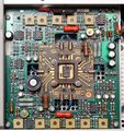
The 7104 makes extensive use of custom integrated circuits and hybrid circuits, inter alia, the 155-0174-00 Delay Line Compensator, 155-0173-00 Vertical Channel Switch, 155-0176-00 Vertical Output Amplifier, 155-0194-00/01/02/03 CRT Termination, 155-0175-00 Trigger Amplifier, 155-0178-00 Horizontal Output Amplifier, 155-0012-00 Z-Axis controller/amplifier, and 155-0067-02 SMPS controller. The high-speed amplifiers use Hypcon ceramic packages that use elastomer-based frames for coupling chip connections to the circuit board at constant impedance. The signal connections are differential throughout, and the signal path was optimized for matching and low reflection, including the plugin to mainframe card-edge connectors and the use of stripline and coplanar waveguide techniques right up to the CRT.
The 7104's amplifiers use a then novel scheme of "feed-beside" compensation (US Pat. 4.132.958) where instead of matching the HF response to the LF response, the LF response is determined by off-the-shelf operational amplifiers in parallel to the high-speed amplifiers, with a number of adjustable R-C time constants to compensate for thermal and other LF effects. The same technique is employed in the 7A29 amplifier plug-in.
Power Supply
The 7104 uses a switch-mode power supply.
Module A23 (schematic page <14>) contains the mains rectifier, base drive circuitry, and power transistors of the inverter (aka, switcher). These transistors produce a 25 kHz waveform that is fed to the primary of T1310, whose secondaries provide the power for the rest of the scope.
Module A24 (also on schematic page <14>) contains the inverter control circuit and rectifiers for the secondaries of T1310. The inverter control circuit uses the 155-0067-02 inverter control IC, which is U1275.
Module A25 (schematic page <15>) contains the low-voltage regulators. There as independently regulated and current-limited sections for the -50V, -15V, +5V, +15V and +50V rails. Each section has an opamp and a BJT output transistor in emitter-follower configuration.
The opamps need power, too. To avoid a dependency cycle, the power supplies for the opamps are separate low-current, low-efficiency zener clamps that in no way depend on the -50V, -15V, +5V, +15V or +50V regulators. The power supplies for the opamps produce -22V, -5.6V, +5.6V, and +22V. To avoid exceeding the opamps' limit of 30V total rail voltage, each opamp either gets -22V and +5.6V, or -5.6V and +22V, depending on whether it needs more output swing in the positive or negative direction.
The +50V section is produces the reference voltage for the other sections. It uses a 9V zener diode, VR1412, as a reference.
Prices
| Year | 1980 | 1984 | 1990 | |
|---|---|---|---|---|
| Mainframe only | Catalog price | $14,400 | $21,380 | $29,995 |
| 2015 value | $41,560 | $48,930 | $54,580 | |
| Mainframe with 7A29, 7A29 Opt. 04, 7B15, 7B10 |
Catalog price | $21,730 | $31,875 | $44,510 |
| 2015 value | $62,700 | $72,960 | $88,990 |
Links
- Hans Springer: 1 GHz at 10 mV in a General Purpose Plug-in Oscilloscope. In TekScope Vol. 11 No. 1, 1979
- Hans Springer's 1979 Electronic Design article on the 7104
- Reading Jim Williams: Scope Sunday 4
- Tek 7104 @ amplifier.cd
- Tek 7104 @ barrytech.com
- A Tektronix oscilloscope that moved faster than light? The Oregonian, 23 Sep 2011. (Original no longer accessible, link via archive.org.)
- Tektronix 7104 @ radiomuseum.org
Pictures
-
-
-
-
-
-
-
-
-
-
-
-
-
-
-
-
-
-
-
-
-
7104 horizontal (top) and vertical (bottom) output amplifiers
-
7104 horizontal output amplifier, CRT connection and termination of distributed horizontal deflection plates
-
7104 vertical channel switch board
-
-
The upper half of the 7104 can be tilted upward for service. A metal support is included, like on the hood of a car.
Measurements
-
Rise time measurement. 150 ps risetime pulse from 067-0587-02 at 100 Hz repetition rate. Measured 240 ps (corrected for 150 ps fixture rise time: 190 ps = 1.8 GHz)
-
Rise time measurement as before, 1000 Hz repetition rate at same brightness settings.
-
7104 recording a single shot pulse (from 067-0587-02) at 200 ps/Div. Camera: Nikon D7000, 50 mm f/1.4, ISO 3200, 1/2 s. CRT filter not removed.
-
7104 recording 1 GHz sine, single shot at 200 ps/Div. Camera: Nikon D7000, 50 mm f/1.4, ISO 3200, 1/2 s. CRT filter not removed. CRT amplification loss is evident around the center line.
-
Faster-than-light beam on 7104? Using a 067-0587-02 calibration fixture at maximum amplitude produces this trace spanning 1.2 Div horizontally at 200 ps/Div and 8 Div vertically. Trace length is (1.2² + 8²)½ × 8.5 mm = 68.8 mm, travelled in 1.2 × 200 ps = 240 ps. Apparent speed is therefore 68.8×10⁻³ / 240×10-12 m/s or 2.86×10⁸ m/s. 95.6% c0 - a very near miss ...


