3S1: Difference between revisions
No edit summary |
No edit summary |
||
| (9 intermediate revisions by 3 users not shown) | |||
| Line 1: | Line 1: | ||
{{Plugin Sidebar | {{Plugin Sidebar | ||
|manufacturer=Tektronix | |||
summary=1 GHz sampling plug-in | | |series=560-series scopes | ||
image=3s1_front.jpg | | |type=3S1 | ||
caption=3S1 | |summary=1 GHz sampling plug-in | ||
introduced=1967 | | |image=3s1_front.jpg | ||
discontinued=(?) | | |caption=Tektronix 3S1 | ||
|introduced=1967 | |||
|discontinued=(?) | |||
* [ | |designers= | ||
* [ | |manuals= | ||
* [[Media:070-0632-00.pdf|Tektronix 3S1 Manual]] | |||
* [[Media:late_3s1_schematics.pdf|Late 3S1 Schematics]] | |||
* [[Media:Tek 3s1 fcp june 1967.pdf|Tektronix 3S1 Factory Cal Procedure 1967]] | |||
* [[Media:Tek 3s1 cal outline.pdf|Tektronix 3S1 Calibration Outline]] (OCR) | |||
}} | }} | ||
The '''Tektronix 3S1''' is a dual-trace [[sampling_oscilloscope|sampling]] plug-in for [[560-series scopes]]. | |||
The '''Tektronix | |||
In many ways, the 3S1 is similar to the [[4S1]], but more compact. | In many ways, the 3S1 is similar to the [[4S1]], but more compact. | ||
The 3S1 provides +100 V and −12.2 V [[ | The 3S1 provides [[probe power|+100 V and −12.2 V]] for [[P6032|P6032 cathode-follower probes]]. | ||
{{BeginSpecs}} | {{BeginSpecs}} | ||
| Line 28: | Line 25: | ||
{{Spec | Bandwidth | 1 GHz (calculated) }} | {{Spec | Bandwidth | 1 GHz (calculated) }} | ||
{{EndSpecs}} | {{EndSpecs}} | ||
==Links== | |||
{{Documents|Link=3S1}} | |||
==Internals== | |||
In contrast to modular sampling plug-ins like the [[3S2]], the 3S1 has built-in sampling heads. | |||
The signal enters through [[GR-874 connector]]s on the front panel. | |||
Each channel has a resistive trigger pickoff followed by a 55 ns coaxial [[delay line]]. | |||
Following the delay line is a compensation circuit designed to (partially) undo the pulse degradation caused by the delay line, and also to provide proper termination for low return loss at the input. | |||
Next in the main signal path is a four-diode sampling bridge driven by a [[snap-off diode]], D73. | |||
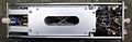
==Pictures== | ==Pictures== | ||
<gallery> | <gallery> | ||
3s1_front.jpg|front view | 3s1_front.jpg|front view | ||
| Line 39: | Line 45: | ||
</gallery> | </gallery> | ||
==Components== | |||
{{Parts|3S1}} | |||
[[Category:Sampling plugins]] | [[Category:Sampling plugins]] | ||
[[Category:560 series plugins]] | [[Category:560 series plugins]] | ||
[[Category:GR874]] | [[Category:GR874]] | ||
Latest revision as of 02:18, 7 March 2024

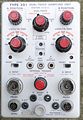
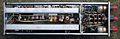
The Tektronix 3S1 is a dual-trace sampling plug-in for 560-series scopes.
In many ways, the 3S1 is similar to the 4S1, but more compact.
The 3S1 provides +100 V and −12.2 V for P6032 cathode-follower probes.
Key Specifications
| Rise Time | 350 ps |
|---|---|
| Bandwidth | 1 GHz (calculated) |
Links
Documents Referencing 3S1
| Document | Class | Title | Authors | Year | Links |
|---|---|---|---|---|---|
| Service Scope 52 Oct 1968.pdf | Article | The State of the Art in Sampling | Al Zimmerman | 1968 | S-1 • S-2 • S-3 • S-4 • S-50 • S-51 • 285 • 3S1 • 3S2 • 3S5 • 3S6 • 3T2 • 3T5 • 3T6 • 3T77A • 568 • 230 |
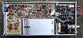
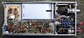
Internals
In contrast to modular sampling plug-ins like the 3S2, the 3S1 has built-in sampling heads. The signal enters through GR-874 connectors on the front panel. Each channel has a resistive trigger pickoff followed by a 55 ns coaxial delay line. Following the delay line is a compensation circuit designed to (partially) undo the pulse degradation caused by the delay line, and also to provide proper termination for low return loss at the input. Next in the main signal path is a four-diode sampling bridge driven by a snap-off diode, D73.
Pictures
-
front view
-
left view
-
right view
-
top view
-
bottom view


Components
Some Parts Used in the 3S1
| Part | Part Number(s) | Class | Description | Used in |
|---|---|---|---|---|
| 151-0261-00 | 151-0261-00 | Discrete component | dual PNP transistor | AM501 • AM502 • CG5001 • CG551AP • FG501 • FG502 • FG503 • OF150 • OF151 • OF152 • OF235 • OS261 • RM502A • R1140 • R5030 • R5031 • R7912 • 067-0679-00 • 067-0807-00 • 1101 • 1140A • 1141 • 1142 • 1350 • 145 • 1450 • 1480 • 1481 • 1482 • 1485 • 1501 • 1801 • 1900 • 1910 • 1980 • 213 • 26A1 • 26A2 • 2620 • 285 • 3A9 • 3A10 • 3S1 • 3S2 • 3S5 • 3S6 • 432 • 434 • 4501 • 454 • 4601 • 4602 • 4610 • 4612 • 4620 • 4632 • 4634 • 4701 • 475 • 492 • 492A • 492AP • 494 • 494P • 496 • 496P • 5A13N • 5A20N • 5A21N • 5A22N • 5A26 • 5L4N • 502A • 5030 • 5031 • 576 • 690SR • 7A22 • 7A29 • 7B51 • 7B71 • 7J20 • 7L5 • 7S11 • 7S12 • 7912AD |