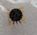
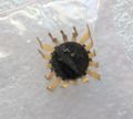
155-0078-00
The 155-0078-xx (M084) is a Tek-made broadband vertical amplifier integrated circuit in a minipac package. The input and output are differential. The 155-0078 and its test fixture were designed by John Addis for the 485 scope (Note 1), which uses no less than 18 of these chips in various grades.
The last two digits of the part number, the grade, correspond to a combination of DC and HF performance. Each M84 was tested for DC performance and HF performance. DC performance was tested using a custom fixture described below. HF performance was tested using the 25ps Push-Pull Pulse Generator.
| SUFFIX | SPEED | DC CHARACTERISTICS | REPLACEABLE BY |
|---|---|---|---|
| 00 | Fast | Best | ---- |
| 01 | Fast | Third best | -03,-00 |
| 02 | Fast | Most relaxed | -01,-03,-00 |
| 03 | Fast | Second best | -00 |
| 04 | Slow | Same as -00 | -00 |
| 05 | Slow | Same as -01 | -03,-00,-07,-04 |
| 06 | Slow | Same as -02 | -01,-03,-00,-05,-07,-04 |
| 07 | Slow | Same as -03 | -00,-04 |
| 10 | Fast | Best | ---- |
| 11 | Fast | Third best | -13,-10 |
| 12 | Fast | Most relaxed | -11,-13,-10 |
| 13 | Fast | Second best | -10 |
| Sometimes an instrument will contain a better grade of part than called for in the manual.
The manual should be consulted for the correct replacement type. | |||
The M84 also comes in 14-pin DIP, as 155-0273-00 and 155-0274-00 (slower grade).
Regarding the various grades of M84, John Addis says:
There are several DC specs which differ with part suffix.
Suffixes -10, -11, -12 and -13 were used for the redesigned M84, known as the M705. The M705 was necessary because the original SH2 (2-2.5GHz?) process was being discontinued. The M705 was designed by Hal Lilliwhite using the faster SH3 process (6-7GHz). Additionally, the M705 apparently had the gain setting resistor laser trimmed at the wafer level. The M705 was designed in late 1989 and tested in early 1990.
There was one high frequency test fixture and perhaps two dc test fixtures. Every M84 was subjected to all tests. All tests were done manually. I designed both test fixtures and the 25ps PPPG.
Transient Response (schematic not shown) uses the 25ps Push Pull Pulse Generator (PPPG) and a sampling scope. Sampler load supplies dc current (through X2 pads and sampler input resistance. The sampling scope chassis is floating at (probably) +5V through 8.2 ohms. 25ps PPPG has transformer coupled trigger output to sampling scope trigger input.
DC test fixture:
I have attached a schematic of a dc test fixture for manufacturing. It looks like this fixture only tests for Vhump. There may have been another test fixture for the other dc tests. Those tests may have been done on a system. The Vhump test may have been so difficult to perform on an automated system that it needed this extra fixture.
Vhump is the amount of maximum dc imbalance, probably referred to the input, which occurs when the variable gain function is swept from full invert to full normal. The two ends of the curve are set to the same dc output level using the balance control attached to pin 1. Ideally, there is no change in dc level under these conditions, but various imbalances in the M84 output devices result in a hump for inverted gain and a hump for the normal gain. Only the -00, -04 and -10 suffixed parts were required to pass this stringent Vhump test. The fixture was in a rubber footed metal chassis about 4” high 5” deep, and 7” wide.
| Displayed Risetime <355ps | -00 and -10 | -01 and -11 | -02 and -12 | -03 and -13 |
| Displayed Risetime 355-410ps | -04 | -05 | -06 | -07 |
| Normal Offset (RTO) | <14mV | <14mV | <28mV | <14mV |
| Invert Offset (RTO) | <14mV | <14mV | <28mV | <14mV |
| HFE of Q1 and Q2 | 70-250 | 70-250 | 50-400 | 70-250 |
| Normal Gain | 2.68-2.96 | 2.68-2.96 | 2.68-2.96 | 2.68-2.96 |
| Invert Gain | 2.68-2.96 | 2.68-2.96 | 2.68-2.96 | 2.68-2.96 |
| Null Offset (Gain = 0) | 10mV | no spec | no spec | <30mV |
| Null Gain (Test of Q3 and Q4) | 14mV | no spec | no spec | <14mV |
| 50% Gain | 0.49-0.51 | no spec | no spec | 0.49-0.51 |
| Off Feedthrough | <0.2mV | <0.2mV | <0.2mV | <0.2mV |
| Normal Hump Voltage | <2.5mV | no spec | no spec | no spec |
| Invert Hump Voltage | <2.5mV | no spec | no spec | no spec |
Pictures
-
Excerpt from 067-0587-01 schematic, showing application of 155-0078-00.
-
155-0078-01 amplifiers in 7A26. Note symmetric layout.
-
M84 Hump Voltage Test Fixture Shematic
-
155-0078-10
-
155-0078-10
Used in
- 475 (U140, U240, U450)
- 485
- 7834, 7844 (U415,U515)
- 7854 (A13U520,A13U590,A13U620,A13U680)
- 7904, 7903 (U5510,U5530,U5550,U5610,U5630,U5650)
- 7912AD, 7912HB
- 7A16A (U350, U450, U550, U750)
- 7A16P (U60240, U60340, U60440, U60540)
- 7A24, 7A26 (U1350,U1450,U1550,U1750,U2350,U2450,U2550,U2750)
- 7A42 (A5U1010,A5U1020,A5U1040,A5U1060)
- 067-0587-01
- AM503
- PG502 (U360, -06)
- DC510 (A12U1311, A12U1331, -10)
Notes
- Note 1: See John Addis quote in 7A11 article


