P7001: Difference between revisions
(Added Bandwidth, design team member, content to external interfaces and display generator) |
(Added description of HSA module) |
||
| Line 78: | Line 78: | ||
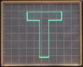
[[File:Tek_P7001_Buspriority.jpg|200px|thumb|right|Bus Priority of a fully equipped P7001]] | [[File:Tek_P7001_Buspriority.jpg|200px|thumb|right|Bus Priority of a fully equipped P7001]] | ||
==Asynchronus Bus== | ===Asynchronus Bus=== | ||
To provide maximum flexibility all P7001 circuit cards are connected over an 16 bit asynchronous bus with 13 address lines. The bus is mostly implemented as etched lines on the Main Interface Board. Only some High speed signals are sent through coaxial cables that connect to the cards using [[Peltola connector]]s. A serially connected line, or daisy chain, in the bus establishes device priority. This signal is called "Data Channel Grant Line". Each card has a specific location in the DPO. The position determines the priority that each card has in the use of the address and data buses. Unused slots must be fitted with a jumper card to close the daisy chain. | To provide maximum flexibility all P7001 circuit cards are connected over an 16 bit asynchronous bus with 13 address lines. The bus is mostly implemented as etched lines on the Main Interface Board. Only some High speed signals are sent through coaxial cables that connect to the cards using [[Peltola connector]]s. A serially connected line, or daisy chain, in the bus establishes device priority. This signal is called "Data Channel Grant Line". Each card has a specific location in the DPO. The position determines the priority that each card has in the use of the address and data buses. Unused slots must be fitted with a jumper card to close the daisy chain. | ||
==Memory== | ===Memory=== | ||
Several types of memory configurations were available: 1k, 2k, 3k or 4k semiconductor memory and also 4k non-volatile core memory. All configurations were available through the whole lifecycle of the P7001. The memory serves to store the acquired waveforms and their associated scale factors. It also stores the computer output for display. Depending on the configuration the following storing capabilites are available: | Several types of memory configurations were available: 1k, 2k, 3k or 4k semiconductor memory and also 4k non-volatile core memory. All configurations were available through the whole lifecycle of the P7001. The memory serves to store the acquired waveforms and their associated scale factors. It also stores the computer output for display. Depending on the configuration the following storing capabilites are available: | ||
| Line 126: | Line 126: | ||
<nowiki>*</nowiki> Removing the Readout-Interface card doubles the space for storing waveforms but eliminates the capability of displaying text information. | <nowiki>*</nowiki> Removing the Readout-Interface card doubles the space for storing waveforms but eliminates the capability of displaying text information. | ||
==Readout Interface== | ===Readout Interface=== | ||
There are two readout devices in the DPO. One is the readout board in the acquisition unit of the 7704A and the other is the readout interface card in the P7001. In the modes "PLUG-INS" or "STORE" all readout information displayed on the CRT come directly from the plugins. In "STORE" mode the readout interface digitizes these information, converts them to ASCII-data and stores it in memory. In the modes "BOTH" or "MEMORY" the readout interface converts the ASCII data back to readout information and displays them on the CRT. | There are two readout devices in the DPO. One is the readout board in the acquisition unit of the 7704A and the other is the readout interface card in the P7001. In the modes "PLUG-INS" or "STORE" all readout information displayed on the CRT come directly from the plugins. In "STORE" mode the readout interface digitizes these information, converts them to ASCII-data and stores it in memory. In the modes "BOTH" or "MEMORY" the readout interface converts the ASCII data back to readout information and displays them on the CRT. | ||
==Display Generator== | ===Display Generator=== | ||
The Display Generator card generates the CRT display of either real-time computer output (XY mode) or data stored in the processsors memory (XT mode). Any combination of the stored and acquired waveforms may be displayed simultaneously. Also, since the display generator operates independent of other devices, changing data may be viewed during a store operation. The Display Generator card has a set of jumpers which switch the CRT output between vector and dot display. | The Display Generator card generates the CRT display of either real-time computer output (XY mode) or data stored in the processsors memory (XT mode). Any combination of the stored and acquired waveforms may be displayed simultaneously. Also, since the display generator operates independent of other devices, changing data may be viewed during a store operation. The Display Generator card has a set of jumpers which switch the CRT output between vector and dot display. | ||
==External Interfaces== | ===Hardware Signal Averager=== | ||
The external interface card provides a bilateral link between the P7001 and an external controller. The controller has full access to all programmable functions in the Processor, and the P7001, in turn, may interrupt the controller at any time. During the production time of the P7001, the following interfaces were developed: | For DPOs which are connected via the fast CP bus, it is no problem to transfer several data sets over the interface and then have the computer calculate the averaged waveform. But with the relatively slow interfaces like GPIB this procedure is impractical. The optional HSA card solves this problem by locally computing the averaged waveform of up to 4096 single waveforms. The HSA card also has the ability to calculate the histogram of a waveform. The histogram will be displayed horizontally at the lower third of the CRT. | ||
===External Interfaces=== | |||
The external interface card provides a bilateral link between the P7001 and an external controller. The controller has full access to all programmable functions in the Processor, and the P7001, in turn, may interrupt the controller at any time. During the production time of the P7001, the following interfaces were gradually developed: | |||
{| class="wikitable" | {| class="wikitable" | ||
Revision as of 12:07, 4 August 2019

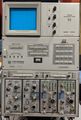
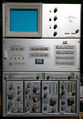
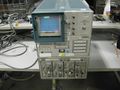
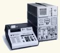
The Tektronix P7001 is a digitizer, processor, and memory for the 7704A oscilloscope. The P7001 can also be connected to an external computer which then is able to process the digitized signals. The complete system was called "Digital Processing Oscilloscope" or "DPO" for short and was presented to the public on 26 March 1973 at the IEEE Intercon in New York City.
The design of the P7001 assumes it will be part of a 7704A system, and that the 7704A will be displaying a steady trace. The vertical and horizonal plug-ins control the beam as they would in any 7000-series scope.
The P7001 periodically samples the horizontal and vertical signals simultaneously as they pass from the plug-ins to the vertical and horizontal amplifiers. This allows it to fill its memory with data points represented as coordinate pairs, (x1,y1), (x2,y2), (x3,y3), etc. It is not necessary that x2 be greater than x1, i.e. the samples can be taken out-of-order with respect to their equivalent time in the waveform.
Key Specifications
| Bandwith | 175MHz |
|---|---|
| Resolution | 10 bit (V), 9 bit (H) |
| Memory | four waveforms, 512 samples each (4K × 10 bit core, or multiple 1k × 10 bit or 2k × 10 bit RAM boards) |
| Sampling rate | 150 kHz ±30 kHz |
| External interface | 16 bit parallel, proprietary "CP bus" (dual 37-pin Sub-D connectors) interfacing with Tektronix CP-1100 or CP-4100 series controllers |
Links
Catalog / Specs
- P7001 Spec 1973
- P7001 Spec 1974
- P7001 Spec 1975
- P7001 Spec 1976
- P7001 Spec 1977
- P7001 Spec 1978
- P7001 Spec 1979
- P7001 Spec 1980
- P7001 Spec 1981
Advertising
Internals
The signal coming from the acquisition unit enters a fast four-diode sample and hold circuit where it is sampled at 150 ksamples/sec. Each sample is digitized using a successive-approximation scheme. The analog to digital converter is made of several chips: a digital to analog converter, a comparator, and control logic.
The P7001 has its own power supply built into it, independent of the power supply in the acquisition unit of the 7704A.
The Acquisition Unit of the 7704A, the P7001 Processor, and the Display Unit of the 7704A are connected by the Acquisition-Processor-Display (APD) Interface.

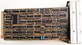
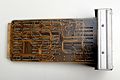
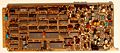
Asynchronus Bus
To provide maximum flexibility all P7001 circuit cards are connected over an 16 bit asynchronous bus with 13 address lines. The bus is mostly implemented as etched lines on the Main Interface Board. Only some High speed signals are sent through coaxial cables that connect to the cards using Peltola connectors. A serially connected line, or daisy chain, in the bus establishes device priority. This signal is called "Data Channel Grant Line". Each card has a specific location in the DPO. The position determines the priority that each card has in the use of the address and data buses. Unused slots must be fitted with a jumper card to close the daisy chain.
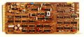
Memory
Several types of memory configurations were available: 1k, 2k, 3k or 4k semiconductor memory and also 4k non-volatile core memory. All configurations were available through the whole lifecycle of the P7001. The memory serves to store the acquired waveforms and their associated scale factors. It also stores the computer output for display. Depending on the configuration the following storing capabilites are available:
| Configuration | Waveforms | Readout Scale factors |
Messages |
|---|---|---|---|
| 1k with readout | 1 | 1 | 3 |
| 1k no readout(*) | 2 | 0 | 0 |
| 2k with readout | 2 | 2 | 4 |
| 2k no readout(*) | 4 | 0 | 0 |
| 3k | 4 | 1 | 4 |
| 4k | 4 | 4 | 12 |
* Removing the Readout-Interface card doubles the space for storing waveforms but eliminates the capability of displaying text information.
Readout Interface
There are two readout devices in the DPO. One is the readout board in the acquisition unit of the 7704A and the other is the readout interface card in the P7001. In the modes "PLUG-INS" or "STORE" all readout information displayed on the CRT come directly from the plugins. In "STORE" mode the readout interface digitizes these information, converts them to ASCII-data and stores it in memory. In the modes "BOTH" or "MEMORY" the readout interface converts the ASCII data back to readout information and displays them on the CRT.
Display Generator
The Display Generator card generates the CRT display of either real-time computer output (XY mode) or data stored in the processsors memory (XT mode). Any combination of the stored and acquired waveforms may be displayed simultaneously. Also, since the display generator operates independent of other devices, changing data may be viewed during a store operation. The Display Generator card has a set of jumpers which switch the CRT output between vector and dot display.
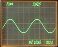
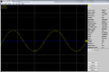
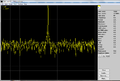
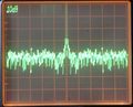
Hardware Signal Averager
For DPOs which are connected via the fast CP bus, it is no problem to transfer several data sets over the interface and then have the computer calculate the averaged waveform. But with the relatively slow interfaces like GPIB this procedure is impractical. The optional HSA card solves this problem by locally computing the averaged waveform of up to 4096 single waveforms. The HSA card also has the ability to calculate the histogram of a waveform. The histogram will be displayed horizontally at the lower third of the CRT.
External Interfaces
The external interface card provides a bilateral link between the P7001 and an external controller. The controller has full access to all programmable functions in the Processor, and the P7001, in turn, may interrupt the controller at any time. During the production time of the P7001, the following interfaces were gradually developed:
| Description | Part Number | Manual |
|---|---|---|
| DPO to Data General Nova | 021-0113-00 | 070-1776-00.pdf |
| DPO to APD (CP Bus) | 021-0116-00 | 070-1654-00.pdf |
| DPO to CP1100 (CP Bus) | 021-0117-00 | 070-1654-01.pdf |
| DPO to TEK31 calculator | 021-0127-00 | 070-1777-00.pdf |
| DPO to CAMAC | 021-0146-00 | |
| DPO to 4010 Family | 021-0175-00 | 070-1936-00.pdf |
| DPO to GPIB | 021-0206-00 | 070-2623-00.pdf |
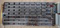
Pictures
-
Front panel
-
P7001 in 7704A
-
P7001 in 7704A
-


Internal
-
Top view
-
Front of backplane
-
main interface board (backplane)
-
Rear of backplane
-
Interunit connector
-
Interunit connector
-
Interunit connector
-

Switching power supply
-
front panel rear
-
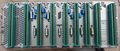
extender boards
-
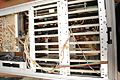
"Dummy-card" or official called "Data Channel Grant jumper card". Needs to be installed in empty slots of Backplane.
-
Data Channel Grant Card
-
Bus Priority of a fully equipped P7001


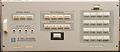
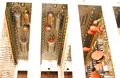
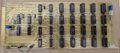
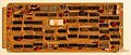
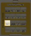
Keyboard overlay cards
-
blank card for user definable programs
-
Two examples of original overlay cards
-
Example of aftermarket overlay cards


External Interfaces (optional)
-
CPBus interface mounted
-
CP Bus Interface front
-
CP Bus Interface rear
-
GPIB Interface IO board
-
GPIB Interface IO board with shielding
-
GPIB Interface CPU board
-
Modern clone of the P7001 GPIB interface
-
Modern clone of the P7001 GPIB interface


Sample and Hold Card
-
Vertical sampling bridge
-
Horizontal sampling bridge
-
Sampling strobe generator
-
Sample and hold edge connector
-
Sample and hold transformers
-
Sample and hold transformer
-
Sample and hold rear


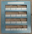
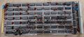
Core Memory (optional)
-
Address decoder
-
Core boards
-
Core memory
-
Core closeup
-
Core closeup
-
High Resolution view of partial core module


Semiconductor memory (optional)
-
2K semiconductor memory (aka "MOS")

ADC and Display
-
Front panel connections
-

ADC
-
ADC rear
-
Probe points on ADC
-
Display generator
-
Display generator rear
-
Z-axis and panel controller
-
Z-axis and panel controller rear
-
Readout interface


Hardware signal Averager (HSA)
-
HSA timing board. The HSA module (optional) performs signal averaging and can calculate a histogram.
-
HSA memory board.


Schematics
-
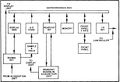
Block Diagram
-

Address map of a fully equipped P7001
-
Power supply schematic 1
-
Power supply schematic 2
-
APD Interconnect


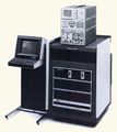
Cofigurations
-
Example of Calculator based system (WP1100) in 1974
-
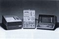
Example of Calculator based system (WP1100) in 1978
-
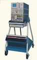
Example of Controller based system (WP1200) in 1973
-
Example of Controller based system (WP1200) in 1975


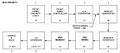
Workflow with connected Controller
-
With pressing a program-call button on the P7001...
-
.. the displayed signal is digitized...
-
...and transferred to the Controller...
-
...the Controller does some calculations...
-
...and transfers the result back to the P7001


X/Y Mode for external Controller
-
A connected computer has direct access to the Display Generator. This allows software-controlled live movements of the Beam.

Design Team
Notable Members of the Design Team were: Hiro Moriyasu, Bruce Hamilton, Luis Navarro, Bob Shand and Jack Gilmore.
-

Key design Team of the P7001.