1240: Difference between revisions
No edit summary |
m (workbook) |
||
| (64 intermediate revisions by 10 users not shown) | |||
| Line 1: | Line 1: | ||
{{ | {{Instrument Sidebar | ||
|class=Logic Analyzer | |||
image= | |manufacturer=Tektronix | ||
caption=Tektronix | |model=1240 | ||
introduced= | |summary=Modular Logic Analyzer | ||
discontinued= | |image=Tek1241 front.jpg | ||
|caption=Tektronix 1241 | |||
|introduced=1984 | |||
* [ | |discontinued=1993 | ||
* [ | |designers= | ||
|manuals= | |||
* [[Media:070-4641-00.pdf|1240 quick start guide]] | |||
* [[Media:070-4340-01.pdf|1240 and 1241 Operator's manual -01]] | |||
* [[Media:070-4340-00.pdf|1240 and 1241 Operator's manual -00]] | |||
* [[Media:070-4342-01.pdf|1240 Service Manual Vol.1]] | |||
* [[Media:070-4717-01.pdf|1240 Service Manual Vol.2]] | |||
* [[Media:070-5378-00.pdf|1241 Service Manual addendum]] | |||
* [[Media:062-6926-00|1240 Seminar Workbook]] | |||
* [[ROM images#1240|ROM images]] | * [[ROM images#1240|ROM images]] | ||
}} | }} | ||
The '''Tektronix 1240''' is a logic analyzer, introduced in 1984. The '''1241''' is the same device but with a color-shutter CRT, it was introduced in 1986. | |||
The | ==Specifications== | ||
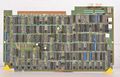
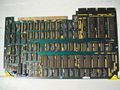
The 1240/1241 accommodate one to four acquisition boards of type [[1240D1]] with 9 channels or [[1240D2]] with 18 channels | |||
for a total of up to 72 acquisition channels. Acquisition speeds reach up to 100 MHz asynchronous or 50 MHz synchronous. | |||
The 1240/41 provides 14 levels of triggering with conditional branching. | |||
The power supply is a switch-mode supply that mainly generates 5 V at up to 45 A. It requires a minimum load of 11.6 A. Additionally it generates 3 V at up to 8 A with no minimum load and several other voltages that are derived from linear post regulators. | There are two cartridge interfaces. | ||
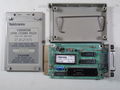
The rear slot is for I/O devices; three were produced. The [[1200C01]] is the RS232C Comm pack. The [[1200C02]] is the GPIB comm pack. The [[1200C11]] is the parallel printer comm pack. It required the [[12RC01]] Printer Support ROM pack. | |||
The cartridge slot interface on the side of the instrument was memory specific and was for ROM and RAM packs. Both 8K and 64K RAM packs with battery backup were made, note that the battery is a potential HazMat made by Catalyst Research and may destroy the cartridge when it leaks. There were also ROM packs (12RMXX series) that allow for mnemonic disassembly and state analysis of most microprocessors of the time. The ROM packs were made with a generic PCB that had two socketed ROMs and jumpers to select the size. | |||
See the [[Microprocessor support table]] for processor configuration options. | |||
There is a design for a multipurpose RAM/ROM pack, called [[Making_1200_series_cartridges|SuperPack]] by Pavel Korensky. Note the errata in the [[Media:Tek1240-SPDesign10.ZIP|README file]]. | |||
It uses either [[P6460]] (general purpose) or [[P6462]] (TTL) 9-channel probes. | |||
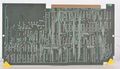
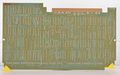
==Internals== | |||
The 1240 is built around an [[Intel 8088]] as the control processor with 64K DRAM, and firmware in a bank of EPROMs. | |||
A separate I/O processor board is powered by a [[Zilog Z-80]]A CPU. The display controller is built from individual TTL and ECL ICs. | |||
The power supply is a switch-mode supply that mainly generates 5 V at up to 45 A. It requires a minimum load of 11.6 A. | |||
Additionally it generates 3 V at up to 8 A with no minimum load and several other voltages that are derived from linear post regulators. | |||
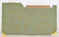
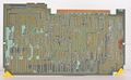
Boards are two to six layers. | |||
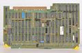
The CPU board has battery backed up RAM to save the current configuration and one user configuration. | |||
This battery is a lithium iodide cell. It will eventually fail and leak, damaging the PCB. | |||
The battery is visible on the picture for the A09 processor board. | |||
==See Also== | |||
* [[Time Stamp]] | |||
==Links== | |||
* [http://www.barrytech.com/tektronix/logic_analyzers/tek1240.html Tektronix 1240] / [http://www.barrytech.com/tektronix/logic_analyzers/tek1241.html 1241] / [http://www.barrytech.com/tektronix/logic_analyzers/tek1240_d2.html 1240D2] @ barrytech.com | |||
* [https://www.youtube.com/watch?v=HzD1hGxzYII Using a 1240] to analyse an 8bit micro. | |||
* [https://www.youtube.com/watch?v=wKR-EUWTZDc Video] showing basic operation of 1241 | |||
* [https://www.youtube.com/watch?v=jq-5DeFpxUM Video] showing GPIB implementation | |||
* [https://spurtikus.de/posts/inside_and_teardown/tektronix-1241-la/ Teardown of a 1241] nice pictures, but the site is in German. | |||
== Pictures == | == Pictures == | ||
<gallery> | <gallery> | ||
Tektronix_1240_front_panel.jpeg | Tektronix 1240, front view | |||
Tektronix_1240_rear_panel.jpeg | Rear panel (note second power switch) | |||
Tek1241 front.jpg | Tektronix 1241 display | |||
Tek 1241 front.jpg | Tektronix 1241, front view | |||
Tek 1241 rear.jpg | Tektronix 1241, rear view | |||
Tektronix_1240_probe_panel.jpeg | Side with probe panel | |||
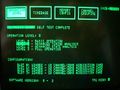
Tek 1240 selftest.jpg | 1240 self test display | |||
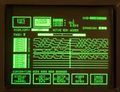
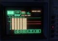
Tek 1240 state view.jpg | 1240 state table view | |||
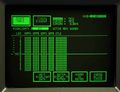
Tek 1240 timing diagram view.jpg | 1240 timing diagram view | |||
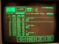
65021240.JPG | 6502 Disassembly | |||
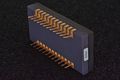
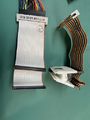
Tek 155-0270-00 from 1240.jpg | Tek [[155-0270-00]] probe data interface hybrid (one of three) | |||
Tek 1240 A06 CRT Drive.jpg | A06 CRT drive board (also includes comms pack interface) | |||
Tek 1240 A06 CRT Drive back.jpg | A06 CRT drive board (rear side) | |||
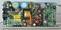
Tek 1240 PSU.jpg | A07 Power supply | |||
Tek 1240 PSU back.jpg | A07 Power supply (rear side) | |||
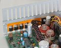
Tek 1240 PSU LV Regulators.jpg | A07 Power supply low voltage regulators | |||
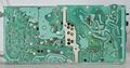
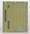
Tek 1240 A08.jpg | A08 Interface board | |||
Tek 1240 A08 back.jpg | A08 Interface board (rear side) | |||
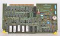
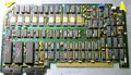
Tek 1240 A09.jpg | A09 Control processor board | |||
Tek 1240 A09 back.jpg | A09 Control processor board (rear side) | |||
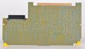
Tek 1240 A10.jpg | A10 I/O processor board | |||
Tek 1240 A10 back.jpg | A10 I/O processor board (rear side) | |||
Tek 1240 A11.jpg | A11 Display generator board | |||
Tek 1240 A11 back.jpg | A11 Display generator board (rear side) | |||
Tek 1240 A14.jpg | A14 Trigger board | |||
Tek 1240 A14 back.jpg | A14 Trigger board (rear side) | |||
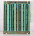
Tek 1240 A15 D1.jpg | A15 1240D1 9-channel board | |||
Tek 1240 A15 D1 back.jpg | A15 1240D1 9-channel board (rear side) | |||
Tek 1240 D2.JPG | 1240D2 | |||
Tek1240-1200C02.jpg | 1200C02 GPIB COMM PACK | |||
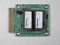
Tek1240-rompack.jpg | ROM PACK | |||
Tek 1241 state view.jpg | 1241 State Table View | |||
1240D1.jpg | 1240D1 | |||
1240D2.jpg | 1240D2 | |||
Tek 1240 accessory 1.jpg | | |||
Tek 1240 accessory 2.jpg | | |||
Tek 1240 accessory 3.jpg | | |||
Tek 1240 accessory 4.jpg | | |||
Tek 1240 accessory 5.jpg | | |||
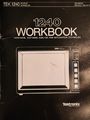
1240 Workbook 062-6926-00 front page.jpg | 1240 Workbook | |||
</gallery> | </gallery> | ||
[[Category:Logic | ==Components== | ||
{{Parts|1240}} | |||
==Plugins== | |||
{{Plugins|1240}} | |||
[[Category:Logic analyzers]] | |||
[[Category:Introduced in 1984]] | |||
[[Category:Parallel printer interface]] | |||
[[Category:RS-232 interface]] | |||
[[Category:GPIB interface]] | |||
Revision as of 07:04, 22 February 2024

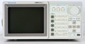
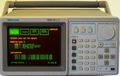
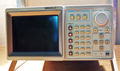
The Tektronix 1240 is a logic analyzer, introduced in 1984. The 1241 is the same device but with a color-shutter CRT, it was introduced in 1986.
Specifications
The 1240/1241 accommodate one to four acquisition boards of type 1240D1 with 9 channels or 1240D2 with 18 channels for a total of up to 72 acquisition channels. Acquisition speeds reach up to 100 MHz asynchronous or 50 MHz synchronous. The 1240/41 provides 14 levels of triggering with conditional branching.
There are two cartridge interfaces.
The rear slot is for I/O devices; three were produced. The 1200C01 is the RS232C Comm pack. The 1200C02 is the GPIB comm pack. The 1200C11 is the parallel printer comm pack. It required the 12RC01 Printer Support ROM pack.
The cartridge slot interface on the side of the instrument was memory specific and was for ROM and RAM packs. Both 8K and 64K RAM packs with battery backup were made, note that the battery is a potential HazMat made by Catalyst Research and may destroy the cartridge when it leaks. There were also ROM packs (12RMXX series) that allow for mnemonic disassembly and state analysis of most microprocessors of the time. The ROM packs were made with a generic PCB that had two socketed ROMs and jumpers to select the size.
See the Microprocessor support table for processor configuration options.
There is a design for a multipurpose RAM/ROM pack, called SuperPack by Pavel Korensky. Note the errata in the README file.
It uses either P6460 (general purpose) or P6462 (TTL) 9-channel probes.
Internals
The 1240 is built around an Intel 8088 as the control processor with 64K DRAM, and firmware in a bank of EPROMs.
A separate I/O processor board is powered by a Zilog Z-80A CPU. The display controller is built from individual TTL and ECL ICs.
The power supply is a switch-mode supply that mainly generates 5 V at up to 45 A. It requires a minimum load of 11.6 A. Additionally it generates 3 V at up to 8 A with no minimum load and several other voltages that are derived from linear post regulators.
Boards are two to six layers.
The CPU board has battery backed up RAM to save the current configuration and one user configuration. This battery is a lithium iodide cell. It will eventually fail and leak, damaging the PCB. The battery is visible on the picture for the A09 processor board.
See Also
Links
- Tektronix 1240 / 1241 / 1240D2 @ barrytech.com
- Using a 1240 to analyse an 8bit micro.
- Video showing basic operation of 1241
- Video showing GPIB implementation
- Teardown of a 1241 nice pictures, but the site is in German.
Pictures
-
Tektronix 1240, front view
-
Rear panel (note second power switch)
-
Tektronix 1241 display
-
Tektronix 1241, front view
-

Tektronix 1241, rear view
-

Side with probe panel
-
1240 self test display
-
1240 state table view
-
1240 timing diagram view
-
6502 Disassembly
-
Tek 155-0270-00 probe data interface hybrid (one of three)
-

A06 CRT drive board (also includes comms pack interface)
-

A06 CRT drive board (rear side)
-
A07 Power supply
-
A07 Power supply (rear side)
-
A07 Power supply low voltage regulators
-
A08 Interface board
-
A08 Interface board (rear side)
-

A09 Control processor board
-
A09 Control processor board (rear side)
-
A10 I/O processor board
-
A10 I/O processor board (rear side)
-
A11 Display generator board
-
A11 Display generator board (rear side)
-
A14 Trigger board
-
A14 Trigger board (rear side)
-

A15 1240D1 9-channel board
-
A15 1240D1 9-channel board (rear side)
-
1240D2
-
1200C02 GPIB COMM PACK
-
ROM PACK
-
1241 State Table View
-

1240D1
-
1240D2
-
-
-
-

-

-
1240 Workbook


Components
Some Parts Used in the 1240
| Part | Part Number(s) | Class | Description | Used in |
|---|---|---|---|---|
| 155-0270-00 | 155-0270-00 | Hybrid integrated circuit | probe data interface | 1240 |
| Intel 8086 | Monolithic integrated circuit | 16-bit microprocessor | 1240 • 2220 • 2221 • 2230 • 2246 • 2232 • 2245A • 4114 • 4115 |
Plugins
Some Plugins compatible with 1240
| Page | Manufacturer | Model | Description | Introduced | Discontinued |
|---|---|---|---|---|---|
| 1200C01 | Tektronix | 1200C01 | RS-232 Comm Pack (interface) | (?) | (?) |
| 1200C02 | Tektronix | 1200C2 | GPIB Comm Pack (interface) | (?) | (?) |
| 1200C11 | Tektronix | 1200C11 | Parallel Printer Comm Pack (interface) | (?) | (?) |
| 1240D1 | Tektronix | 1240/D1 | 9-channel input card | (?) | (?) |
| 1240D2 | Tektronix | 1240D2 | 18-channel input card | (?) | (?) |
| 12R01 | Tektronix | 12R01 | Performance Analysis ROM Pack | (?) | (?) |
| 12RC01 | Tektronix | 1200C11 | Printer Support ROM Pack | (?) | (?) |
| 12RM01 | Tektronix | 12RM01 | Disassembler ROM Pack (Intel 8080) | (?) | (?) |
| 12RM02 | Tektronix | 12RM02 | Disassembler ROM Pack (Intel 8085) | (?) | (?) |
| 12RM03 | Tektronix | 12RM03 | Disassembler ROM Pack (Intel 8086) | (?) | (?) |
| 12RM04 | Tektronix | 12RM04 | Disassembler ROM Pack (Intel 8088) | (?) | (?) |
| 12RM05 | Tektronix | 12RM05 | Disassembler ROM Pack (Intel 80186) | (?) | (?) |
| 12RM06 | Tektronix | 12RM06 | Disassembler ROM Pack (Intel 80188) | (?) | (?) |
| 12RM08 | Tektronix | 12RM08 | Disassembler ROM Pack (Intel 80286) | (?) | (?) |
| 12RM21 | Tektronix | 12RM21 | Disassembler ROM Pack (Motorola 6800) | (?) | (?) |
| 12RM22 | Tektronix | 12RM22 | Disassembler ROM Pack (Motorola 6802) | (?) | (?) |
| 12RM23 | Tektronix | 12RM23 | Disassembler ROM Pack (Motorola 6808) | (?) | (?) |
| 12RM24 | Tektronix | 12RM24 | Disassembler ROM Pack (Motorola 6809) | (?) | (?) |
| 12RM25 | Tektronix | 12RM25 | Disassembler ROM Pack (Motorola 68000) | (?) | (?) |
| 12RM26 | Tektronix | 12RM26 | Disassembler ROM Pack (Motorola 68008) | (?) | (?) |
| 12RM27 | Tektronix | 12RM27 | Disassembler ROM Pack (Motorola 68010) | (?) | (?) |
| 12RM31 | Tektronix | 12RM31 | Disassembler ROM Pack (Motorola 68020) | (?) | (?) |
| 12RM33 | Tektronix | 12RM33 | Disassembler ROM Pack (Motorola 68030) | (?) | (?) |
| 12RM41 | Tektronix | 12RM41 | Disassembler ROM Pack (Zilog Z-80) | (?) | (?) |
| 12RM42 | Tektronix | 12RM42 | Disassembler ROM Pack (Zilog Z8001) | (?) | (?) |
| 12RM43 | Tektronix | 12RM43 | Disassembler ROM Pack (Zilog Z8002) | (?) | (?) |
| 12RM62A | Tektronix | 12RM62A | Disassembler ROM Pack (Fairchild F9450) | (?) | (?) |
| 12RM63 | Tektronix | 12RM63 | Disassembler ROM Pack (MOS Technology 6502) | (?) | (?) |
| 12RM71 | Tektronix | 12RM71 | Disassembler ROM Pack (National Semiconductor NSC800) | (?) | (?) |
| 12RM99 | Tektronix | 12RM99 | Disassembler ROM Pack | (?) | (?) |
| 12RS01 | Tektronix | 12RS01 | 8K RAM Pack | (?) | (?) |
| PM201 | Tektronix | PM201 | Intel 8086/8088 personality module | (?) | (?) |
| PM202 | Tektronix | PM202 | Intel 80186/80188 personality module | (?) | (?) |
| PM203 | Tektronix | PM203 | Motorola 68000/08/10 personality module | (?) | (?) |
| PM204 | Tektronix | PM204 | Intel 80286 personality module | 1985 | (?) |
| PM205 | Tektronix | PM205 | Motorola 68020 personality module | (?) | (?) |