M377
The Tektronix M377 (P/N 165-2129-03,165-2089-06,155-2089-05) is an amplifier monolithic integrated circuit designed by John Addis.
Its initial use was in the 11A16, 11A32, 11A33, 11A34 and 11A52 plug-ins.
About the M377, John Addis says:
The M377 was a single-channel plugin on a chip with 0 V common mode input and output voltages, excellent variable gain control, two four-pole bandwidth limits, and three outputs which could be separately inverted and turned on or off.
It was the first wideband analog IC with level shift on chip (allowing 0 V common mode input and output and without PNP transistors), first wideband amplifier with any on-chip bandwidth limit selection, first to have more than two fixed gain settings (it has six), first to require only one transient response adjustment (no thermals), and the first to have a highly linear relationship between a control voltage and gain. It also had excellent overdrive recovery.
(See also John's comments on the M777 successor.)
Later, the M377 and M777 were also used in several other Tek instruments. If the instrument has more than 300 MHz bandwidth at 1 mV/div sensitivity, it can be assumed to be using the M777 which makes use of Tek's later IC fabrication process that provides transistors with higher ft.
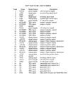
The M377 and M777 are in the following instruments based on the specified bandwidth at 1 mV/div:
| 2245 | 2245A | 2247 | 2247A | 2252 |
| AM503A | AM503B | |||
| TDS410 | TDS420 | TDS460 | ||
| TDS520 | TDS520A | TDS524A | ||
| TDS540 | TDS540A | TDS544A | ||
| TDS620B | TDS644B | |||
| TDS654C |
| TDS520B | TDS520C | TDS520D | TDS540B | TDS540C | TDS540D | TDS580D |
| TDS680B | TDS680C | TDS684A | TDS684B | TDS684C | ||
| TDS714L | TDS724A | TDS724C | TDS724D | TDS744A | TDS754C | TDS754D |
| TDS784A | TDS784C | TDS784D |
Links
- John Addis, Versatile Analogue Chip for Oscilloscope Plug-ins. Electronic Engineering, London, August/September 1988.
- M377 Component Specification
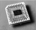
Packaging of the M377
11000 series instruments and the AM503A and AM503B use a 1.22 cm square, flat ceramic package compatible with the Hypcon connector. The ceramic rests on a heat sink supplied by the instrument’s chassis.
TDS series oscilloscopes use a J lead package with a tall heat sink (155-0378-00/01). The package is soldered to the circuit board.
The 200 Ω output impedance of the version for the four-channel 11A34 (50 Ω resulting with four paralleled outputs) is achieved in the laser trimming stage of wafer production.
Tek part numbers:
| Instrument | Instrument SN range | Part Number | Output R/side | Components on ceramic hybrid |
|---|---|---|---|---|
| 11A32 | B010100 - B031028 | 165-2089-03 | 100 Ω | M377 chip only |
| 11A32 | B031029 - up | 165-2089-05 | 100 Ω | M377 chip only |
| 11A33 | B010101 - up | 165-2089-05 | 100 Ω | M377 chip only |
| 11A34 | B010100 - B031044 | 165-2089-04 | 200 Ω | M377 chip only |
| 11A34 | B031045 - up | 165-2089-06 | 200 Ω | M377 chip only |
| 11A52 | B010100 - B010179 | 165-2129-02 | 100 Ω | Diode bridge + 50 Ω input R + M377 chip |
| 11A52 | B010180 - up | 165-2129-03 | 100 Ω | Diode bridge + 50 Ω input R + M377 chip |
| AM503A | B010101 - up | 165-2456-00 | 100 Ω | M377 chip only aka M694 (relaxed DC bal spec) |
| AM503B | B010101 - up | 165-2456-00 | 100 Ω | M377 chip only aka M694 (relaxed DC bal spec) |
Output Control Signals
The M377 has one input (differential) and three differential outputs which are identical circuits. Each output has a its own control pins for:
- Output invert
- Output enable. When an output is disabled, it has no offset and maintains the specified termination impedance. That is, the internal parallel output termination remains connected, but the signal current is shut off. The self-calibration of 11k systems makes use of this property.
- High-frequency adjustment. The HF ADJ pins have 2 kΩ input resistance to ground. The nominally acceptable inputs are ±1 V to ground. Because the input resistance tracks the nichrome standard resistors inside the chip, the input is actually current sensitive, not that it makes much difference. This current affects the standing current in a feedback amplifier and hence its open loop gain. At low frequencies, the gain of the M377 is determined entirely by resistor values. At high frequencies, there is phase shift and changing the open loop gain will also change the closed loop gain, hence the transient response.
Var Gain Control Signal
The M377 has a single VAR GAIN control input, which affects all three outputs. This control signal has a range of −1 V to +1 V. −1 V results in 0 gain. +1 V results in full gain.
165-2089-xx Pinout
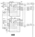
In the 11A32, 11A34, and 11A52, pairs of 165-2089-xx IC are placed on the board so that their outputs are facing one another, allowing their outputs to be wired in parallel with a minimum of board complexity and asymmetry. The purpose of the three output channels varies depending on the rotational orientation of the IC on the board.
- Output 1 (pins 25 and 26) is either AUX SIG (aka AUX TRIGGER) or DISPLAY,
- Output 2 (pins 22 and 23) of all 165-2089-xx ICs are the TRIGGER signal.
- Output 3 (pins 19 and 20) is either AUX SIG (aka AUX TRIGGER) or DISPLAY.

Two 165-2089-xx M377 ICs facing one another in an 11A52. Output 1 of U310 is in parallel with output 3 of U410. Output 3 of U310 is in parallel with output 1 of U410.
Note that in the 11A32 and 11A34, the HF ADJUST control voltages are not set identically for the three outputs. The reason for this is that the DISPLAY and TRIGGER outputs are in parallel with the corresponding output from another M377, which forms a broadband termination. In contrast, the AUX SIG outputs are not combined, and therefore have ¼ W resistors on the PCB, shunting to ground. The ¼ W resistors become inductive at high frequencies, so the optimal HF adjustment for the AUX SIG output is different than for the DISPLAY and TRIGGER outputs.
|
|
|
Pin function legend
Power pins Ground pins HF signals TTL digital control signals analog control signals
Pictures
-
M377 in an 11A52, as U310 and U410. Each M377 chip has a differential output impedance of 200 Ω. The two chips' outputs are in parallel, driving the output pins of the plug-in with a differential impedance of 100 Ω, or 50 Ω per side.
-
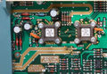
Two M377 chips (packaged as part number 165-2129-03) in an 11A52
-
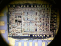
M377 die
-
-
M377 Die pad names and numbers


