Distributed deflection plates


In CRTs, a trade/off exists between writing rate, deflection sensitivity and spot size. For example, a slower beam improves the sensitivity but hurts writing rate and spot size due to mutual repulsion between electrons. Within a given technology (e.g. mono acceleration, post deflection acceleration or microchannel plate (MCP)), these three characteristics can be traded off against each other. Improve one and one or both of the others suffer. Improve the technology and all three can be improved simultaneously. Writing rate is important for observing single short-lived events, but is not important for repetitive signals. Spot size is important in showing detail in the waveform. Sensitivity is important mostly to permit greater bandwidth in vertical amplifiers.
Construction of high-performance CRTs
Post-deflection acceleration was probably the first technology change. It dates from the early 1950s and was a major factor in the success of the 530/540 series of oscilloscopes. Post-deflection acceleration is exactly what its name implies: After the electron beam travels through both vertical and horizontal deflection plates, the beam is accelerated by a resistive helix painted on the inside of the tube from near the deflection plates almost to the phosphor screen. The end near the deflection plates is held at the potential of the plates. This assures that the electrons do not see the high voltage at the phosphor screen and can travel between the plates relatively slowly, allowing them to be deflected easily. After passing though the plates, the resistive helix presents an increasing voltage that gives the electrons a much higher speed, resulting in a bright spot. Since the electrons move quickly, they disperse less due to their mutual repulsion, resulting in a small spot size. This was the standard until the early 1960s.
Shaped metal meshes placed after the deflection plates provide magnification and shield the deflection plates from the strength of the post-acceleration field but scatter the electrons and thus hurt spot size.
In the 1980s, electron lenses were introduced – metal structures that are located after the deflection plates, but unlike meshes do not intersect the electron beam and do not scatter electrons. These lenses nevertheless magnify spot size along with beam deflection. Both meshes and lenses do, however, contribute net performance by isolating the deflection structure from the acceleration potential. Two types of lenses were used, the box lens (in the 7104) and later the quadrupole lens.
Effect of distributed deflection plates
All CRTs have a finite frequency response, but distributed deflection plates extend the CRT's bandwidth as well as aid the vertical amplifier by virtually eliminating the capacitive load on the vertical amplifier.
Even a CRT with a single pair of deflection plates has a frequency response that is not as simple as an RLC circuit. A voltage step applied to a single pair of deflection plates simultaneously affects all the electrons between the plates at the time of the step. Those electrons that are just exiting the plates see no deflection as they continue on their way to the phosphor for display. Those that are at the entrance to the plates feel the effects of all voltage changes that take place during their transit through the plates. Therefore they bear the memory of any deflection plate voltage changes during their journey through the plates. The effects of any deflection plate voltage changes are delayed in proportion to their distance from the exit simply because it takes time for the electrons to travel from the entrance to exit of the plates. This is what makes the frequency response so complicated.
For example, if it takes 1 ns for an electron to travel the length of the plates (usually one on each side of the electron beam) and a 1 GHz sine wave is applied between the plates, the full 360 degrees of the sine wave causes the electron to move up and down during transit. By the time the electron exits the plate 1 ns later, the electron is back where it started from. There is no net deflection and the sensitivity is zero at this frequency.
Making the transit time shorter by shortening the deflection plates increases the bandwidth, but reduces the deflection sensitivity by the same factor. Using a distributed deflection plate structure is a way around this, extending the bandwidth without reducing the deflection sensitivity. The only trade off is in complexity and therefore cost.
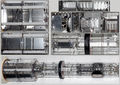
In the distributed deflection plate structure, the original deflection plates are cut up into individual segments. The capacitance of the deflection plates can then be made part of a lumped delay line by adding inductance between each of the plate segments. These inductors are usually inside the CRT.
Signals in any lumped delay line travel relatively slowly compared with the speed of light. If done correctly, the electron beam velocity can equal the signal velocity down the lumped delay line. The signal and electrons travel together. This reduces the time the electron beam spends between any particular deflection plate pair by the number of plates. Therefore the electrons react to the same electric field no matter where they are along the structure.
The higher the required bandwidth, the more likely the distributed deflection plate structure will physically look like a uniform transmission line than separate plates connected by wires.
Termination
The lumped delay line is usually terminated at the end of the deflection structure outside the CRT. The end of this delay line needs to be terminated to prevent the drive signal from being reflected back through the line. In Tektronix scopes, the termination resistor can often be seen attached to a second pair of vertical deflection terminals on the side of the CRT, which bring out the end of the transmission line. This means the vertical amplifier is driving a resistive load and not the capacitance of a long deflection plate. In some scopes (e.g. the 7104), even the output impedance of the vertical amplifier is equal to the CRT characteristic impedance. While this is not essential, it does reduce incidental reflections.
The termination resistor is outside the CRT because the transient response is cleanest when the termination is adjustable, and a laser trimmed resistor inside the tube would contaminate the tube's vacuum.
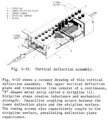
Note that the last deflection plates are often tilted and farther apart than the others. This is to prevent the deflection plates from intercepting and cutting off the electron beam at large deflections. The famous 545A's CRT, which does not have distributed deflection plates, has only 4 divisions of deflection because of vertical deflection plate interception.
Reality
As a generalization, oscilloscopes with 100 MHz bandwidth or less do not have a distributed deflection structure. (The 580-series scopes with a distributed deflection structure and a 100 MHz bandwidth is an exception).
A real deflection plate structure is slightly limited by the fact that the last deflection plates may be longer and more widely separated than the others. Furthermore, the characteristic impedance of the deflection plate structure may not be identical to that of the leads going into and out of the CRT. These are usually high impedance lines and difficult to make.
Higher frequency deflection structures use more deflection plates that are closer together. Electrically they look more like transmission lines and some are traveling wave structures. For example, the 7104 deflection structure is called a box helix. The identical top and bottom deflection plates are both constructed as a ribbon wound into a square helix. Through the middle of each helix is a square metal tube, the ground plane. Each deflection plate has a characteristic impedance of 100 ohms, which is mostly determined by the ground plane inside the helix.
At high frequencies, each turn of the helix electromagnetically couples with the next turn down the line, causing the signal to jump ahead slightly. As the frequency goes up, the coupling increases causing an increase in the wave's velocity. This "velocity dispersion" causes the electron beam and the signal to be spatially separated at high frequencies, to the detriment of the frequency response.

History
Distributed deflection plates were introduced in the 580-series scopes in the late 1950s. Transistorized scopes followed with the upgrade of the 50 MHz 453 to the 150 MHz model 454 in 1967.
Typically, only the vertical deflection plates are distributed. An exception is the 7103/7104 due to the high horizontal system bandwidth required (350 MHz).
| Model | Distributed Y plates | Distributed X plates |
|---|---|---|
| 11301, 11302 | yes | no |
| 2445, 2465 | yes | no |
| 2467 | yes | no |
| 453 | no | no |
| 454 | yes | no |
| 465 | no | no |
| 475 | yes | no |
| 485 | yes | no |
| 519 | yes | no |
| 53x, 54x, 55x | no | no |
| 56x | no | no |
| 581/A, 585/A | yes | no |
| 647/A | no | no |
| 7403 | no | no |
| 7503, 7504 | no | no |
| 7603 | no | no |
| 7612D | no | no |
| 7704, 7704A | yes | no |
| 7844 | yes | no |
| 7854 | yes | no |
| 7904, 7904A, 7903 | yes | no |
| 7912 | yes | no |
| 7104, 7103 | yes | yes |
| 7250 | yes | yes |
| SCD1000, SCD5000 | yes | yes |
Literature
- Cliff Moulton, US Patent 2,922,074, Electron Beam Deflection Structure
- Peter Keller, The Cathode-Ray Tube: Technology, History, and Applications, . Palisades Press, 1991. ISBN 0963155903, 9780963155900
- Oscilloscope Cathode-Ray Tube Concepts, Chuck Devere, 1969
- John Addis, Good Engineering and Fast Vertical Amplifiers, in Jim Williams (Ed.), Analog Circuit Design: Art, Science and Personalities (1991), p.115+
- Aris Silzars, Richard Knight, The Deflection Sensitivity of Traveling-Wave Electron-Beam Deflection Structures (Nov 1972) IEEE Transactions on Electron Devices
-
Distributed deflection plates in 154-0850-01 CRT (2445,2455)
-
-
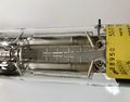
Deflection system of 519 scope
-