11401: Difference between revisions
(stub page) |
No edit summary |
||
| (49 intermediate revisions by 4 users not shown) | |||
| Line 1: | Line 1: | ||
{{Oscilloscope Sidebar | |||
|manufacturer=Tektronix | |||
|series=11000-series scopes | |||
|model=11401 | |||
|summary=Digitizing scope | |||
|image=Tek 11401 front.jpg | |||
|caption=Tek 11401 | |||
|introduced=1986 | |||
|discontinued=1989 | |||
|designers=Tom Rousseau | |||
|manuals= | |||
* [[Media:070-6103-00.pdf|11401/11402 Introduction Manual]] | |||
* [[Media:070-6255-00.pdf|11401/11402 Programmers Quick Reference]] | |||
* [[Media:070-6779-03.pdf|11401 and 11402 Service Reference]] (OCR) | |||
* [[Media:070-7386-99.pdf|Tektronix 11401 and 11402 Extended Service Manual Volume 1]] | |||
* [[Media:070-7387-99.pdf|Tektronix 11401 and 11402 Extended Service Manual Volume 2]] | |||
Using random equivalent time sampling, it can acquire up to eight channels at 300 MHz, six channels at 600 MHz, or up to 3 channels at 1 GHz. | * ''please add free user manual'' (070-5791-00) | ||
* ''see [[11402]]/[[11403]] for manuals of sister models'' | |||
* [[Category:Manual needed]] ''please add service manual'' | |||
* [[Media:070-6640-00.pdf|11401 11402 Firmware Upgrade Instructions]] (OCR) | |||
* [[Media:The 11400 story.pdf|Story of 11400 Development]] | |||
* [[Media:Tek 11401 URM 101087.pdf|Tektronix 11401 User Reference Manual with Firmware Update]] (OCR) | |||
{{ROM Images}} | |||
}} | |||
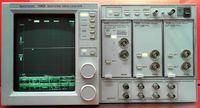
The '''Tektronix 11401''' is a 500 MHz digitizing scope with three plugin bays | |||
accepting [[:Category:11000 series plugins|11000-series plugins]]. | |||
The 11401 and [[11402]] (which has 1 GHz bandwidth) differ only in their sampler board. | |||
In all other respects, the 11401 and 11402 are the same. | |||
Project manager of the 11400 series was [[Tom Rousseau]], who was also project manager for the [[7854]]. | |||
The 11400 engineering team included some of the main people from the [[7854]] project. | |||
The assistant project manager and person responsible for the touch panel and display was [[Murlan Kaufman]]. | |||
<!-- Using random equivalent time sampling, it can acquire up to eight channels at 300 MHz, six channels at 600 MHz, or up to 3 channels at 1 GHz. --> | |||
The 11401 mainframe uses equivalent time sampling at a rate of 20 MHz (20 Msps). | |||
Each sample has 10 bits of resolution. | |||
It is capable of displaying eight separate 10 bit resolution traces at one time. | |||
The mainframe is fully remotely programmable over [[RS-232]] or [[GPIB]]. | |||
This mainframe accepts up to three plugins with differing numbers of channels and bandwidths. | |||
For example, each [[11A52]] plugin allows two inputs at 500 MHz bandwidth (50 Ω only input impedance). | |||
The [[11A34]] plugin allows four inputs at 300 MHz bandwidth, and the [[11A32]] allows two channels at 300 MHz. | |||
Three 11A34 plugins then allow up to 12 channels of information, | |||
but the mainframe limits the number displayed at any one time to eight. | |||
The other four channels may still be used for triggering. | |||
The [[11402]] and (later) [[11403]] and [[DSA600]] mainframes allow up to 1 GHz of bandwidth | |||
with an [[11A71]] with one 50 Ω input, or two 50 Ω inputs in the (later) [[11A72]]. | |||
{{MissingSpecs}} | |||
Resolution is up to 10 ps horizontal and 10 bits vertical, with 10,240 points of memory. | Resolution is up to 10 ps horizontal and 10 bits vertical, with 10,240 points of memory. | ||
== | ==Internals == | ||
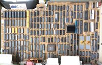
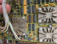
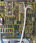
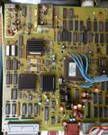
Note: The photos of the "Prototype 11401" are of a scope that said [[11331]] on the front panel. | |||
The 11401 uses the [[156-2622-00]] [[SDI]] controller IC (U330). | |||
=== Vertical Signal Path === | |||
Each of the three plug-in bays in the 11401 has a dedicated sampler. | |||
The sampling clock is common to the three samplers. | |||
The sampling pulse is generated by an ECL 2-input OR gate being fed SAMPLE_CLOCK and delay_5ns(invert(SAMPLE_CLOCK)). | |||
This produces 5 ns pulses with rise time around 1 ns, which are fed to a discrete NPN differential pair operating | |||
in a clipping current-switch mode, resulting in faster edges. | |||
The output of the differential pair drive a strobe generator IC, U1040, which is an M453 die, | |||
packaged as part number [[155-0320-00]] or 155-0320-01, depending on the mainframe's serial number. | |||
U1040 has three sampling strobe outputs, which are fed to the sampling gates. | |||
The plug-in connector's differential "DISPLAY" pins are connected to the samplers by coaxial cable, | |||
i.e. there are no high-speed amplifiers in the mainframe's signal path. | |||
The DISPLAY+ and DISPLAY- signals are fed to separate samplers. | |||
The sampled signals are combined in the channel switch to obtain a single-ended signal that is fed to the ADC. | |||
The outputs of the sampling gates are multiplexed by a channel switch into an ADC. | |||
A two-stage pipelined ADC (Tek part number [[155-0289-01]]) is used, with five bits per stage. | |||
Each stage has a bank of 32 comparators. | |||
The output of the ADC is stored in RAM. | |||
The contents of the RAM may have many points depending on the size of the acquisition window. | |||
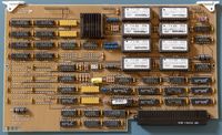
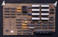
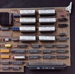
The "Waveform Compressor" board takes the contents of the acquisition RAM and renders it to 512 points on the horizontal axis for display. | |||
==Links== | ==Links== | ||
* http://www.barrytech.com/tektronix/tek11000/tek11401.html | * [http://www.barrytech.com/tektronix/tek11000/tek11401.html Tek 11401 @ barrytech.com] | ||
==See Also== | |||
* [[Media:Case study 11401 11402 werner.pdf|Sidebar on 11401 and 11402 in May 1987 IEEE Spectrum]] | |||
==Pictures== | ==Pictures== | ||
<gallery> | <gallery widths="200" heights="150"> | ||
Tek 11401 front.jpg | |||
Tek 11401.jpg | |||
Early 11401 lvpsu diagnostic leds.jpg |Prototype 11401 LV PSU diagnostic LEDs | |||
Early 11401 lvpsu control rectifier.jpg |Prototype 11401 LV PSU Control Rectifier | |||
Early 11401 lv lspsu inverter.jpg |Prototype 11401 LV PSU Inverter | |||
Early 11401 timebase board.jpg |Prototype 11401 TImebase Board | |||
Early 11401 trigger 155-0239-02.jpg |Prototype 11401 Trigger 155-0239-02 | |||
Early 11401 acquisition board right.jpg |Prototype 11401 acquisition board right | |||
Early 11401 acquisition board left.jpg |Prototype 11401 acquisition board left | |||
Early 11401 acquisition board.jpg |Prototype 11401 acquisition board | |||
Early 11401 bottom internal.jpg |Prototype 11401 bottom internal | |||
11401_A13-MOTHERBOARD_PROD.jpg |Production 11401 A13 / Mother Board | |||
Early 11401 bus signals.jpg |Prototype 11401 A13 signal test points | |||
Early 11401 bus socket.jpg |Prototype 11401 A13 bus sockets | |||
Early 11401 bus.jpg |Another view of the Prototype 11401 A13 bus sockets | |||
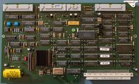
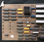
11401_A16-WAVEFORMCOMPRESSOR_PROD.jpg |Production 11401 A16 / Waveform Compressor board. Board referred to as 670-8859-00. | |||
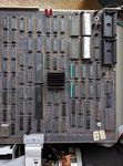
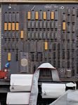
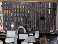
Early 11401 waveform compressor front.jpg |Prototype 11401 A16 board | |||
Early 11401 waveform compressor back.jpg |Prototype 11401 A16 board rear | |||
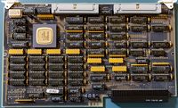
11401_A15-MMU_PROD.jpg |Production A15 / Memory Management Unit. Board referred to as 670-8858-00. | |||
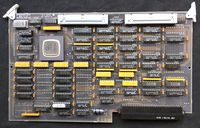
Early 11401 670-8858 board front.jpg |Prototype 11401 A15 board | |||
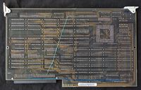
Early 11401 670-8858 board back.jpg |Prototype 11401 A15 board rear | |||
11401_A14-IO_PROD.jpg |Production 11401 A14 / I/O board. Board referred to as 670-8854-00. | |||
Early 11401 io board front.jpg |Prototype 11401 I/O board | |||
Early 11401 io board back.jpg |Prototype 11401 I/O board rear | |||
Early 11401 display side.jpg |Prototype 11401 display side | |||
Early 11401 display top.jpg |Prototype 11401 display top | |||
11401_A17-MAINPROCESSOR_PROD.jpg |Production 11401 A17 / Main Processor board. Board referred to as 670-8855-00. | |||
Early 11401 670-8855 board front.jpg |Prototype 11401 A17 board | |||
Early 11401 670-8855 board rear.jpg |Prototype 11401 A17 board rear | |||
Early 11401 1562472-00.jpg |Prototype 11401 1562472-00 | |||
11401_A18-MEMORYBD_PROD.jpg |Production 11401 A18 / Memory board, lacking the memory expansion option. | |||
Early 11401 memory board front.jpg |Prototype 11401 A18 / Memory board | |||
Early 11401 memory board rear.jpg |Prototype 11401 A18 board rear | |||
Early 11401 memory board front right.jpg |Prototype 11401 A18 board front right | |||
Early 11401 memory board front left.jpg |Prototype 11401 A18 board front left | |||
Early 11401 display controller right.jpg |Prototype 11401 display controller right | |||
Early 11401 display controller left.jpg |Prototype 11401 display controller left | |||
Early 11401 display controller.jpg |Prototype 11401 display controller | |||
Early 11401 top internal.jpg |Prototype 11401 top internal | |||
Tek 11401 right.jpg |11401 right side | |||
Tek 11401 rear.jpg |11401 rear | |||
</gallery> | </gallery> | ||
==Components== | |||
{{Parts|11401}} | |||
[[Category:11000 series mainframes]] | [[Category:11000 series mainframes]] | ||
[[Category:RS-232 interface]] | |||
[[Category:GPIB interface]] | |||
Latest revision as of 05:40, 3 July 2024
The Tektronix 11401 is a 500 MHz digitizing scope with three plugin bays accepting 11000-series plugins. The 11401 and 11402 (which has 1 GHz bandwidth) differ only in their sampler board. In all other respects, the 11401 and 11402 are the same.
Project manager of the 11400 series was Tom Rousseau, who was also project manager for the 7854. The 11400 engineering team included some of the main people from the 7854 project. The assistant project manager and person responsible for the touch panel and display was Murlan Kaufman.
The 11401 mainframe uses equivalent time sampling at a rate of 20 MHz (20 Msps). Each sample has 10 bits of resolution. It is capable of displaying eight separate 10 bit resolution traces at one time. The mainframe is fully remotely programmable over RS-232 or GPIB.
This mainframe accepts up to three plugins with differing numbers of channels and bandwidths. For example, each 11A52 plugin allows two inputs at 500 MHz bandwidth (50 Ω only input impedance). The 11A34 plugin allows four inputs at 300 MHz bandwidth, and the 11A32 allows two channels at 300 MHz. Three 11A34 plugins then allow up to 12 channels of information, but the mainframe limits the number displayed at any one time to eight. The other four channels may still be used for triggering. The 11402 and (later) 11403 and DSA600 mainframes allow up to 1 GHz of bandwidth with an 11A71 with one 50 Ω input, or two 50 Ω inputs in the (later) 11A72.
Key Specifications
- please add
Resolution is up to 10 ps horizontal and 10 bits vertical, with 10,240 points of memory.
Internals
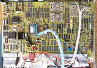
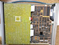
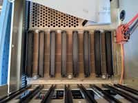
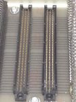
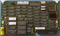
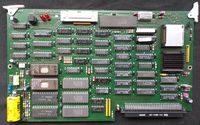
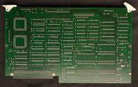
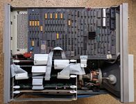
Note: The photos of the "Prototype 11401" are of a scope that said 11331 on the front panel.
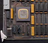
The 11401 uses the 156-2622-00 SDI controller IC (U330).
Vertical Signal Path
Each of the three plug-in bays in the 11401 has a dedicated sampler. The sampling clock is common to the three samplers.
The sampling pulse is generated by an ECL 2-input OR gate being fed SAMPLE_CLOCK and delay_5ns(invert(SAMPLE_CLOCK)). This produces 5 ns pulses with rise time around 1 ns, which are fed to a discrete NPN differential pair operating in a clipping current-switch mode, resulting in faster edges. The output of the differential pair drive a strobe generator IC, U1040, which is an M453 die, packaged as part number 155-0320-00 or 155-0320-01, depending on the mainframe's serial number. U1040 has three sampling strobe outputs, which are fed to the sampling gates.
The plug-in connector's differential "DISPLAY" pins are connected to the samplers by coaxial cable, i.e. there are no high-speed amplifiers in the mainframe's signal path. The DISPLAY+ and DISPLAY- signals are fed to separate samplers. The sampled signals are combined in the channel switch to obtain a single-ended signal that is fed to the ADC.
The outputs of the sampling gates are multiplexed by a channel switch into an ADC. A two-stage pipelined ADC (Tek part number 155-0289-01) is used, with five bits per stage. Each stage has a bank of 32 comparators.
The output of the ADC is stored in RAM. The contents of the RAM may have many points depending on the size of the acquisition window. The "Waveform Compressor" board takes the contents of the acquisition RAM and renders it to 512 points on the horizontal axis for display.
Links
See Also
Pictures
-
-
-
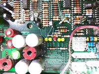
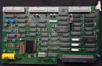
Prototype 11401 LV PSU diagnostic LEDs
-
Prototype 11401 LV PSU Control Rectifier
-
Prototype 11401 LV PSU Inverter
-
Prototype 11401 TImebase Board
-
Prototype 11401 Trigger 155-0239-02
-
Prototype 11401 acquisition board right
-
Prototype 11401 acquisition board left
-
Prototype 11401 acquisition board
-
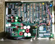
Prototype 11401 bottom internal
-
Production 11401 A13 / Mother Board
-
Prototype 11401 A13 signal test points
-
Prototype 11401 A13 bus sockets
-
Another view of the Prototype 11401 A13 bus sockets
-
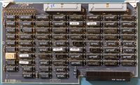
Production 11401 A16 / Waveform Compressor board. Board referred to as 670-8859-00.
-
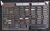
Prototype 11401 A16 board
-
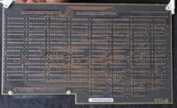
Prototype 11401 A16 board rear
-
Production A15 / Memory Management Unit. Board referred to as 670-8858-00.
-
Prototype 11401 A15 board
-
Prototype 11401 A15 board rear
-
Production 11401 A14 / I/O board. Board referred to as 670-8854-00.
-
Prototype 11401 I/O board
-
Prototype 11401 I/O board rear
-
Prototype 11401 display side
-
Prototype 11401 display top
-
Production 11401 A17 / Main Processor board. Board referred to as 670-8855-00.
-
Prototype 11401 A17 board
-
Prototype 11401 A17 board rear
-
Prototype 11401 1562472-00
-
Production 11401 A18 / Memory board, lacking the memory expansion option.
-
Prototype 11401 A18 / Memory board
-
Prototype 11401 A18 board rear
-
Prototype 11401 A18 board front right
-
Prototype 11401 A18 board front left
-
Prototype 11401 display controller right
-
Prototype 11401 display controller left
-
Prototype 11401 display controller
-
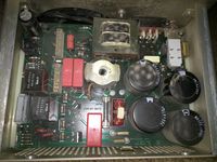
Prototype 11401 top internal
-
11401 right side
-
11401 rear
Components
Some Parts Used in the 11401
| Part | Part Number(s) | Class | Description | Used in |
|---|---|---|---|---|
| 155-0239-00 | 155-0239-00 • 155-0239-01 • 155-0239-02 | Hybrid integrated circuit | trigger | 2424L • 2430 • 2430A • 2432 • 2445 • 2465 • 2467 • 2400-series scopes • 11201 • 11401 • 11402 |
| 155-0282-00 | 155-0282-00 | Monolithic integrated circuit | D/A converter | 11201 • 11401 • TSG-170 • TSG-271 |
| 155-0320-00 | 155-0320-00 | Monolithic integrated circuit | sampling strobe generator | 11401 |
| 155-0349-00 | 155-0349-00 | Monolithic integrated circuit | custom | 11201 • 11401 |
| 165-2065-02 | 165-2065-02 | Hybrid integrated circuit | Time Interpolator | 11201 • 11401 • 11402 |
| Intel 80286 | Monolithic integrated circuit | 16-bit microprocessor | 11201 • 11401 • 11402 | |
| Intel 80287 | Monolithic integrated circuit | floating-point coprocessor | 11201 • 11401 • 11402 |

