155-0032-00: Difference between revisions
No edit summary |
No edit summary |
||
| Line 3: | Line 3: | ||
|Model=M55 | |Model=M55 | ||
|Part_nos=155-0032-00,155-0032-01 | |Part_nos=155-0032-00,155-0032-01 | ||
|Description=variable-gain transconductance amplifier | |Description=variable-gain transconductance (current output with voltage input) amplifier | ||
|Used_in=335;464;465;465B;466;475;475A;475M;634;650;651;652;653;655;656;670;671;7A12;475;FG504;1440;1460;1480;1481;1482;1485 | |Used_in=335;464;465;465B;466;475;475A;475M;634;650;651;652;653;655;656;670;671;7A12;475;FG504;1440;1460;1480;1481;1482;1485 | ||
|Designers=Roy Hayes;Einar Traa | |Designers=Roy Hayes;Einar Traa | ||
}} in a 16-pin DIP | }} in a 16-pin DIP. The [[155-0216-00]] and [[155-0217-00]] (M55D aka M055D) appear to be improved successor versions. | ||
Regarding the 155-0032-xx, [[John Addis]] says, | Regarding the 155-0032-xx, [[John Addis]] says, | ||
<blockquote> | <blockquote> | ||
The 155-0032-00’s IC process had an FT of 1.0 | The 155-0032-00’s IC process had an FT of 1.0 GHz, rather inadequate for the job, but that was all there was at the time. | ||
The on-chip resistors were diffused and thus had too poor a TC and tolerance for use as gain-setting resistors. | The on-chip resistors were diffused (there were no thin film resistors in that process) and thus had too poor a TC and tolerance for use as gain-setting resistors. | ||
As you can see, there are two separate gain | As you can see, there are two separate gain choices determined by which set of emitters is chosen, pins 1 and 16 or 2 and 15. | ||
This selection is made off chip by choosing Q205 or Q215 to carry the current through R212. | This selection is made off chip by choosing Q205 or Q215 to carry the current through R212. | ||
Pot R217 allows dc balance at 5 mV/div to match that at all other sensitivities, controlled elsewhere. | Pot R217 allows dc balance at 5 mV/div to match that at all other sensitivities, controlled elsewhere. | ||
| Line 19: | Line 19: | ||
Pin 12 ultimately selects which pair of the four output cross-connected transistors passes | Pin 12 ultimately selects which pair of the four output cross-connected transistors passes | ||
the signal current from the two transistors whose bases are connected to pin 4. | the signal current from the two transistors whose bases are connected to pin 4. | ||
Which pair of output transistors is chosen determines the polarity of the output signal. | Which pair of output transistors is chosen determines the polarity choice of the output signal (Normal or Invert). | ||
This same pair of transistors also enables variable gain by allowing a controlled amount of cross-coupling of the signal. | This same pair of transistors also enables variable gain by allowing a controlled amount of cross-coupling of the signal. | ||
| Line 34: | Line 34: | ||
The M377 was a single channel plugin on a chip with 0 V common mode input and output voltages, | The M377 was a single channel plugin on a chip with 0 V common mode input and output voltages, | ||
very linear variable gain control, two four pole bandwidth limits, three outputs which could be individually inverted and turned on or off. | |||
The M377 was the first wideband analog IC with dc level shift on chip (allowing 0 V common mode input and output and without PNP transistors), the | |||
first wideband amplifier with any on-chip bandwidth limit selection, first to have more than two fixed gain settings (it has six), | first wideband amplifier with any on-chip bandwidth limit selection, first to have more than two fixed gain settings (it has six), | ||
and first to require only one transient response adjustment (no thermals), and the first to have a highly linear relationship | and first to require only one transient response adjustment (no thermals), and the first to have a highly linear relationship | ||
Revision as of 21:16, 10 September 2024
The Tektronix M55 (P/N 155-0032-00,155-0032-01) is a variable-gain transconductance (current output with voltage input) amplifier monolithic integrated circuit in a 16-pin DIP. The 155-0216-00 and 155-0217-00 (M55D aka M055D) appear to be improved successor versions.
Regarding the 155-0032-xx, John Addis says,
The 155-0032-00’s IC process had an FT of 1.0 GHz, rather inadequate for the job, but that was all there was at the time. The on-chip resistors were diffused (there were no thin film resistors in that process) and thus had too poor a TC and tolerance for use as gain-setting resistors.
As you can see, there are two separate gain choices determined by which set of emitters is chosen, pins 1 and 16 or 2 and 15. This selection is made off chip by choosing Q205 or Q215 to carry the current through R212. Pot R217 allows dc balance at 5 mV/div to match that at all other sensitivities, controlled elsewhere.
Pin 12 ultimately selects which pair of the four output cross-connected transistors passes the signal current from the two transistors whose bases are connected to pin 4. Which pair of output transistors is chosen determines the polarity choice of the output signal (Normal or Invert). This same pair of transistors also enables variable gain by allowing a controlled amount of cross-coupling of the signal.
This is an undesirable way of doing variable gain control, but neither Roy nor I knew that at the time. It is a noisy configuration. At the 0% signal gain there is lots of noise gain. It has poor thermal balance at anything other than 100% and the not very useful 0% signal gain. In between 0% and 100% gain, the circuit is poor in noise and thermal balance.
I went on to use the same (Gilbert Multiplier) circuit in the 155-0078-xx (M84) and made the same bad choice again in the 7A29. In our defense, with just two stages and the need to do both invert and variable gain control somewhere, there was not a lot of choice.
It was not until I designed the M377 for the 11000 series of plugins (11A32, 11A33, 11A34, 11A52) that I finally got it right. (See the British magazine Electronic Engineering, September, 1988, pp 40-41.)
The M377 was a single channel plugin on a chip with 0 V common mode input and output voltages, very linear variable gain control, two four pole bandwidth limits, three outputs which could be individually inverted and turned on or off.
The M377 was the first wideband analog IC with dc level shift on chip (allowing 0 V common mode input and output and without PNP transistors), the first wideband amplifier with any on-chip bandwidth limit selection, first to have more than two fixed gain settings (it has six), and first to require only one transient response adjustment (no thermals), and the first to have a highly linear relationship between a control voltage and gain. It also had excellent overdrive recovery. Live and learn.
The input differential amplifier's emitters are brought out to pins 1 and 16. Off-chip components provide frequency compensation and determine the gain. The chip has an input to select normal or inverted phase and an input to vary the "position", i.e., output current offset.
- Pin 1: emitter current source
- Pin 2: gain switching
- Pin 3: input balance
- Pin 4: bias
- Pin 5: −8 V
- Pin 6: position current source
- Pin 7: ground
- Pin 8: signal out −
- Pin 9: signal out +
- Pin 10: position
- Pin 11: +8 V
- Pin 12: norm / -inv
- Pin 13: +5 V
- Pin 14: signal in −
- Pin 15: gain switching
- Pin 16: emitter current source
Used in
- The 155-0032-00 is used in the front end of the 335 signal path, just after a JFET high-impedance buffer. It is discussed on page 3-5 of the 335 manual.
- The 155-0032-00 is also used as the trigger amplifier in the 465. In this application, the input differential amplifier has a total tail current of about 11 mA.
- The 155-0032-00 is used as a vertical gain stage in the 7A12.
- 475 (U520, U720)
- FG504 (U770) below SN B057720
- 1440 (-01), 1460 (-01), 1478 (-01)
- 1480, 1481, 1482, 1485
- 464, 465, 465B, 466, 475, 475A, 475M
- 634, 650, 651, 652, 653, 655, 656, 670, 671
- See also 155-0217-00
Some instruments using part 155-0032-00
| Instrument | Manufacturer | Class | Model | Description | Introduced |
|---|---|---|---|---|---|
| 1440 | Tektronix | Audio/Video | 1440 | Automatic Video Corrector | 1974 |
| 1480 | Tektronix | Audio/Video | 1480 | NTSC waveform monitor | 1976 |
| 1481 | Tektronix | Audio/Video | 1481 | PAL Waveform Monitor | 1977 |
| 1482 | Tektronix | Audio/Video | 1482 | PAL-M Waveform Monitor | (?) |
| 1485 | Tektronix | Audio/Video | 1485 | TV waveform monitor | (?) |
| 335 | Sony/Tektronix | Oscilloscope | 335 | Compact dual-trace 35 MHz oscilloscope | 1976 |
| 464 | Tektronix | Oscilloscope | 464 | Portable 100 MHz dual-trace storage scope | 1975 |
| 465 | Tektronix | Oscilloscope | 465 | Portable 100 MHz dual-trace scope | 1972 |
| 465B | Tektronix | Oscilloscope | 465B | Portable 100 MHz dual-trace scope | 1980 |
| 466 | Tektronix | Oscilloscope | 466 | Portable 100 MHz dual-trace storage scope | 1974 |
| 475 | Tektronix | Oscilloscope | 475 | Portable 200 MHz dual-trace scope | 1972 |
| 475 | Tektronix | Oscilloscope | 475 | Portable 200 MHz dual-trace scope | 1972 |
| 475A | Tektronix | Oscilloscope | 475A | Portable 250 MHz dual-trace scope | 1977 |
| 634 | Tektronix | Oscilloscope | 634 | Video CRT Monitor | 1978 |
| 650 | Tektronix | Audio/Video | 650HR | NTSC color video monitor | 1971 |
| 651 | Tektronix | Display | 651 | PAL color video monitor | 1972 |
| 652 | Tektronix | Display | 652 | PAL-M color video monitor | 1973 |
| 655 | Tektronix | Display | 655 | NTSC/PAL color video monitor | 1972 |
| 656 | Tektronix | Display | 656 | SECAM color video monitor | (?) |
| 7A12 | Tektronix | Plug-in | 7A12 | 120 MHz dual-channel amplifier | 1969 |
| FG504 | Tektronix | Plug-in | FG504 | 40 MHz function generator | 1976 |
Datasheet
Diagrams
-

155-0032-01
-

155-0032-01
-

155-0032-01
-

Block diagram
-
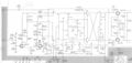
155-0032-00 schematic shown in the 7A12 schematic
-
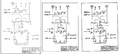
Comparison of 155-0032-00, 155-0216-00, and 155-0217-00 diagrams


