DL502: Difference between revisions
(cat) |
No edit summary |
||
| (9 intermediate revisions by 3 users not shown) | |||
| Line 1: | Line 1: | ||
{{TM500 | mfg=Tektronix | type=DL502 | function=digital latch| class=digital function | image=Tek dl502 1.JPG | introduced=1978 | discontinued=1984 | | |||
designers= |manuals= | |||
* [[Media:070-2397-00.pdf|Tektronix DL502 Manual (PDF)]] | |||
* [http://w140.com/DD501-DL502-WR501.pdf Catalog Descriptions of DD501, DL502, and WR501 (PDF)] | * [http://w140.com/DD501-DL502-WR501.pdf Catalog Descriptions of DD501, DL502, and WR501 (PDF)] | ||
}} | |||
It is used with the [[7D01]] or [[LA501W]] logic analyzers to detect narrow pulses in a data stream that cannot be detected by the logic analyzer alone. | |||
The DL502 has two inputs for [[P6451]] 8+1 channel probes and two output cables with the same connectors as the probes, to plug into the 7D01's inputs. Additionally the "Store Clock Out" connector of the [[7D01]] needs to be connected to the "Store Clock In" connector of the DL502. | |||
When paired with a [[LA501W]] the output connectors plug into the [[WR501]] that is part of the [[LA501W]] bundle. The [[LA501W]] must be modified with the [[012-0725-01|LA501W Clock Access Conversion Kit]] to provide the necessary clock for the "Store Clock In" connector of the DL502. | |||
{{BeginSpecs}} | |||
{{Spec |Number of channels | 16}} | |||
{{Spec |Minimum pulse width | 5ns}} | |||
{{Spec |Minimum clock period | 20ns}} | |||
{{EndSpecs}} | |||
==Links== | |||
{{Documents|Link=DL502}} | |||
{{PatentLinks|DL502}} | |||
==Pictures== | |||
<gallery> | <gallery> | ||
Tek dl502 1.JPG | |||
DL502_catalog.jpg |catalog image | |||
Dl502 description.png|description | |||
</gallery> | </gallery> | ||
Latest revision as of 05:18, 6 October 2024
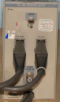
The Tektronix DL502 is a digital latch plug-in for the TM500 system.
It is used with the 7D01 or LA501W logic analyzers to detect narrow pulses in a data stream that cannot be detected by the logic analyzer alone.
The DL502 has two inputs for P6451 8+1 channel probes and two output cables with the same connectors as the probes, to plug into the 7D01's inputs. Additionally the "Store Clock Out" connector of the 7D01 needs to be connected to the "Store Clock In" connector of the DL502.
When paired with a LA501W the output connectors plug into the WR501 that is part of the LA501W bundle. The LA501W must be modified with the LA501W Clock Access Conversion Kit to provide the necessary clock for the "Store Clock In" connector of the DL502.
Key Specifications
| Number of channels | 16 |
|---|---|
| Minimum pulse width | 5ns |
| Minimum clock period | 20ns |
Links
Documents Referencing DL502
| Document | Class | Title | Authors | Year | Links |
|---|---|---|---|---|---|
| Tekscope 1977 V9 N3.pdf | Article | New Products | 1977 | FEM181 • DL2 • DL502 • 851 | |
| 070-2088-04.pdf | Book | TM500 Series Rear Interface Data Book | 1985 | AA501 • AF501 • AM501 • AM502 • AM503 • AM511 • DC501 • DC502 • DC503 • DC503A • DC504 • DC505 • DC505A • DC508 • DC508A • DC509 • DC510 • DC5009 • DC5010 • DD501 • DL502 • DM501 • DM501A • DM502 • DM502A • DM505 • DM5010 • FG501 • FG501A • FG502 • FG503 • FG504 • FG507 • FG5010 • LA501 • LA501W • WR501 • MR501 • PG501 • PG502 • PG505 • PG506 • PG507 • PG508 • PS501 • PS502 • PS503 • PS503A • PS505 • PS5010 • RG501 • SC501 • SC502 • SC503 • SC504 • SG502 • SG503 • SG504 • SG505 • SW503 • TG501 • TR501 • TR502 • MI5010 • MX5010 • SI5010 |
Pictures
-
-
catalog image
-
description


