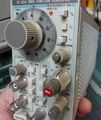
FG501A
The Tektronix FG501A is a function generator plug-in for the TM500 system.

The FG501A replaced the FG501 (1972) in 1981.
Key Specifications
| Frequency | 0.002 Hz to 2 MHz in eight decade steps |
|---|---|
| Output | Max. 30 Vp-p (into high impedance) |
| Attenuator | 60 dB in 20 dB steps, 20 dB variable |
| Rise time | 25 ns |
| Features | symmetry variable from 5 to 95% |
| Signals | sine, square, triangle, ramp, pulse |
| Features |
|
The TRIG OUT signal is available on the front panel via a BSM female connector.
The Phase control is effective in gated mode to control the starting phase of the generated waveform.
Differences to FG501
The FG501 non-A frequency maximum is 1 MHz, while the "A" model is specified at 2 MHz.
The FG501 features seven different functions – sine, triangle, square, positive- and negative-going ramps, pulse ≤50% duty, and pulse ≥50%. The duration of ramp and pulse waveforms is always equal to the half-cycle time of the sine, square, or triangle waveform frequency.
The FG501A model provides only three functions – sine, triangle, and square. However, it has an added variable symmetry control, effectively allowing the same functionality as the non-A model.
The FG501A also adds an output attenuator and increases the maximum open-circuit output voltage to 30 V from the FG501's 10/15 V.
Links
- FG507 - same specs as FG501A, added internal sweep generator
- Zenwizard Studios - Tektronix FG501A Repair and Calibration/Alignment
Documents Referencing FG501A
| Document | Class | Title | Authors | Year | Links |
|---|---|---|---|---|---|
| 070-2088-04.pdf | Book | TM500 Series Rear Interface Data Book | 1985 | AA501 • AF501 • AM501 • AM502 • AM503 • AM511 • DC501 • DC502 • DC503 • DC503A • DC504 • DC505 • DC505A • DC508 • DC508A • DC509 • DC510 • DC5009 • DC5010 • DD501 • DL502 • DM501 • DM501A • DM502 • DM502A • DM505 • DM5010 • FG501 • FG501A • FG502 • FG503 • FG504 • FG507 • FG5010 • LA501 • LA501W • WR501 • MR501 • PG501 • PG502 • PG505 • PG506 • PG507 • PG508 • PS501 • PS502 • PS503 • PS503A • PS505 • PS5010 • RG501 • SC501 • SC502 • SC503 • SC504 • SG502 • SG503 • SG504 • SG505 • SW503 • TG501 • TR501 • TR502 • MI5010 • MX5010 • SI5010 |
Patents that may apply to FG501A
| Page | Title | Inventors | Filing date | Grant date | Links |
|---|---|---|---|---|---|
| Patent US 3562464A | Cam actuated switch having movable and fixed contacts on circuit board | Howard Vollum • Willem H Verhoef • Tony Sprando | 1968-10-07 | 1971-02-09 | Cam switches • 1501 • 2101 • 2701 • 2703 • 432 • 434 • 465 • 475 • 5A15N • 5A18N • 5A20N • 5A21N • 5A38 • 5A45 • 5B10N • 5B12N • 7A15 • 7A16A • 7A18 • 7A19 • 7A24 • 7A26 • 7B10 • 7B15 • 7B50 • 7B51 • 7B52 • 7B53A • 7B50A • 7B70 • 7B71 • 7B80 • 7B85 • 7B87 • 7B92 • 7B92A • 7D01 • 7D12 • 7D15 • 7J20 • 7S12 • 7T11 • 7T11A • AF501 • AM502 • AM503 • DC502 • DC503 • DC504 • DC505 • DM501 • DM502 • FG501 • FG501A • FG502 • FG503 • FG504 • FG507 • PG501 • PG502 • PG505 • PG506 • PG506A • PG508 • TG501 • SC502 • SC503 • SC504 |
Rear Interface
- Output: 28A (Common 27A)
- Trigger Output: 27B (Common 28B)
- Gate/Trigger Input: 24B (Common 25B)
- VCF Input: 21B (Common 22B)
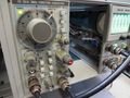
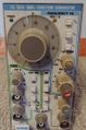
Pictures
-
-
-
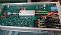
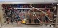
right interior
-
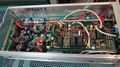
left interior
-
-

right interior
-
left interior
-

rear connector


Components
Some Parts Used in the FG501A
- (no results)