AM503
The Tektronix AM503 is a current probe amplifier plug-in for the TM500 system.
Versions AM503A and AM503B have digital readout of deflection factor. The AM503S is an AM503A bundled with a TM502A mainframe, a TM-500 toolbox, and a A6302 probe.
The current probe input is an Amphenol 165-12 connector. It contains pins for hall element and transformer connections, lock detection, probe degaussing, and probe type encoding.
The AM503, AM5030 and 11A16 use the same connector.
Key Specifications
| Bandwidth | |
|---|---|
| Sensitivity |
|
| Range |
|
| Output | into 50 Ω scope input set to 10 mV/div |
| Power | 17 W |
| Compatible probes |
Rear interface
The output can be detached from the front panel BNC socket which has a Peltola connector on the inside, and re-attached to a Peltola socket near the top of the interface connector, where it is terminated in 50 Ω and brought out on pin 28A (ground on 27A).
Background
Regarding the AM503, Dale Dorando says:
The AM503 was a redesign of the 6042 current probe from 1967. It was initially going to be an oscilloscope plug-in. About 80% through the project design a new line of products was started called TM500. It was requested that we change the design to be a TM500 plug-in module instead. The AM503 front panel still looks like a scope’s plug-in. The AC/DC switch and 5 MHz bandwidth switch, for example, were left on the front panel from the oscilloscope design. There are still some remnants of the oscilloscope circuits, such as the cam switch that interfaced to a circuit board that sets the scope’s readout in amps/div. The square pin header connector on the back of the circuit board was for the readout, but not used. The high frequency amplifier was differential to accommodate an oscilloscope’s differential input. The last change was the output stage that was added to convert the differential circuit to single ended, and then output that to a front panel BNC.
The AM503 was also intended to work with future higher frequency probes, like the P6022 with an added hall device for DC measurements. The smaller P6022 had a 120 MHz bandwidth, whereas the P6302 was only 50 MHz. The design engineer (actually only an R&D technician) moved to the TM500 engineering and evaluation group before this probe was created. The AM503 was being developed in the Accessories division in Beaverton, since that’s where the other current probes were designed. That was unusual as all the other plug-ins were being designed by the TM500 group on Walker Road, near Hillsboro. The AM503 was one of the first plug-ins for the TM500 line of products. It required more power than the current plug-in designs so the transformer and supply were changed in the TM500 frames early on just for the AM503.
There were some innovations that were incorporated in this design: The cam switch with replaceable laser trimmed attenuator resistors, a 1 GHz Gilbert cell op amp (actually developed by Howard Jones in 1963). This IC, 155-0078-xx, was being developed by Tek’s IC department. (At the same time these IC designers were teaching the technology at the University of Portland as part of Tek’s excellent education and training program.) The Peltola connector, developed by Tek’s Ron Peltola, a very low cost connector that worked well, even for the highest frequencies. A BNC was adapted to be used with the Peltola and is used on the front panel.
A large section of the AM503 was basically duplicating the front end of an oscilloscope since that was the original design intent, so it was thought later that the differential amp section could be eliminated and the amplifier made much smaller and even become part of a standalone probe. A prototype was created (author’s senior project at the University of Portland) but shelved, as there was no longer an engineer in Accessories for current probes. Much later it gave rise to the TCP series of stand-alone current probes.
The P6302 and P6303 probes utilized a Hall device that was manufactured in the clean room of the Accessories Manufacturing group. It was deposited onto a bar of ferrite that was later assembled into a U shape with other ferrite and potted in a mu-metal can along with the transformer bobbins. The Hall device used for the DC measurements used a vacuum deposition process with indium antimonide. The cores were lapped and polished to a few Fresnel lines flatness to minimize the gap on the sliding ferrite. The L/R time constant affects the point where the Hall device and coils’ bandwidths crossover.
An interesting aspect of the design was trying to find a way to test and calibrate the peak current pulse on the larger P6303. Luckily we had the tube lab. We developed an argon filled thyratron that could discharge a 4 kV charge line into a 4 Ω load. The load resistor was designed and built by Tektronix. A large rectangular ceramic plate was coated with a metal film resistor. It had a voltage divider tap to allow for a safer measurement point. It was laser trimmed for accuracy. The current probe would measure the current to ground through this resistor, so the voltage was near zero for the user. The 4 kV supply was charged into a 4 Ω transmission line so a clean high current pulse would be generated. This concept was taken from Tek’s 109 pulse generator.
A trigger circuit was designed to fire the grid. It was based on the xenon flash circuit of the C5 camera flash, also in the Accessories group. The first prototype I made arced across the laser trim lines in the metal film resistor as they were cut perpendicular to the current flow. This caused high voltage gradients across the film and thus the arcing across the cuts. We changed the laser trim to be parallel to the current path along the outside edges. That’s what was used in manufacturing for calibrating the risetime of the P6303.
Also interesting, the P6303 required special potting epoxy developed by 3M. The epoxy used in other current probes put excessive stress on the larger ferrite that caused the inductance to drop to zero due to the magnetostriction property of ferrite. The epoxy could even also cause shear fractures in the ferrite.
Links
Pictures
AM503
-
AM503 front
-
AM503 left side
-
AM503 right side
-
AM503
-
AM503
-
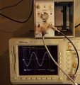
AM503 feeding a TDS744A
-
AM503 Special Adapter
AM503A
-
AM503A
AM503B
-
AM503B
-
Two AM503B in a TM502A
-
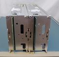
Rear view of two AM503B plug-ins
-
PCB component side
-
PCB soldering side
-
Ceramic daughter board with relays
-
2nd daughter board
-
Tek specific IC
See also
- AM5030
- http://www.tek.com/datasheet/current-measurement-system-probes
- Current Probe Simulator 067-0802-99
Custom ICs used in the AM503
| Page | Model | Part nos | Description | Designers | Used in |
|---|---|---|---|---|---|
| 155-0078-00 | M084 | 155-0078-xx • 155-0273-00 • 155-0274-00 | broadband amplifier | John Addis | 464 • 465 • 466 • 468 • 475 • 475A • 475M • 485 • 7834 • 7844 • 7854 • 7904 • R7903 • R7912 • 7912AD • 7912HB • 7104 • 7A16A • 7A16P • 7A24 • 7A26 • 7A42 • 067-0587-01 • 067-0680-00 • AM503 • PG502 • PG508 • DC510 • DC5010 • FG5010 |


