DC503: Difference between revisions
Jump to navigation
Jump to search
No edit summary |
No edit summary |
||
| (5 intermediate revisions by 2 users not shown) | |||
| Line 1: | Line 1: | ||
{{TM500 | mfg=Tektronix | type=DC503 | function=100 MHz, 7-digit frequency counter | class=counter | image= | {{TM500 | mfg=Tektronix | type=DC503 | function=100 MHz, 7-digit frequency counter | class=counter | image=DC503 early operating.jpg | introduced=1972 | discontinued=1981 | ||
|designers=Roland Crop;Jim Geddes | |designers=Roland Crop;Jim Geddes | ||
|manuals= | |manuals= | ||
| Line 5: | Line 5: | ||
* [[Media:Tek_DC503_M23275-1_Improved_Channel_A_Triggering.pdf|DC503 M23275-1 Improved Ch A Triggering]] | * [[Media:Tek_DC503_M23275-1_Improved_Channel_A_Triggering.pdf|DC503 M23275-1 Improved Ch A Triggering]] | ||
* [[Media:050-1276-00.pdf|DC501, DC502, DC503 Service Note 050-1276-00]] | * [[Media:050-1276-00.pdf|DC501, DC502, DC503 Service Note 050-1276-00]] | ||
* [[Media:Tek_DC503_FCP_1977-02-18.pdf|Tektronix DC503 Factory Calibration Procedure]] (OCR) | * [[Media:Tek_DC503_FCP_1977-02-18.pdf|Tektronix DC503 Factory Calibration Procedure]] (OCR) | ||
}} | }}. It was [[introduced in 1972]] at the launch of the TM500 system, and superseded by the [[DC503A]] in 1981. | ||
Opt.01 is an [[wikipedia:Crystal oven|OCXO]] for improved stability. | Opt.01 is an [[wikipedia:Crystal oven|OCXO]] for improved stability. | ||
{{BeginSpecs}} | {{BeginSpecs}} | ||
{{Spec | Resolution | 7 digits}} | |||
{{Spec | Frequency Range | 0.1 Hz (AC coupled: 10 Hz) to 100 MHz }} | {{Spec | Frequency Range | 0.1 Hz (AC coupled: 10 Hz) to 100 MHz }} | ||
{{Spec | Impedance | 1 MΩ paralleled by approx. 20 pF}} | {{Spec | Impedance | 1 MΩ paralleled by approx. 20 pF}} | ||
{{Spec | Sensitivity | 300 mV<sub>p-p</sub> sinewave times attenuation to 100 MHz }} | {{Spec | Sensitivity | 300 mV<sub>p-p</sub> sinewave times attenuation to 100 MHz }} | ||
{{Spec | Max Input Voltage | | {{Spec | Max Input Voltage, 1× Att. | 50 V @ ≤2 kHz, derate –20 dB/decade to 10 MHz; 10 V @ 10 kHz to 25 MHz, derate –20 dB/decade to 50 MHz; 5 V @ 50 MHz to 100 MHz }} | ||
{{Spec | Max Input Voltage | {{Spec | Max Input Voltage, 10×/100× Att. | 500 V @ ≤2 MHz, derate –20 dB/decade to 100 MHz }} | ||
{{SpecGroup | Standard time base }} | {{SpecGroup | Standard time base }} | ||
{{Spec | Frequency | 1 MHz ± 1 × 10<sup>-7</sup> at cal }} | {{Spec | Frequency | 1 MHz ± 1 × 10<sup>-7</sup> at cal }} | ||
| Line 26: | Line 25: | ||
{{Spec | Error | ≤ ±5 × 10<sup>-7</sup> from 0 °C to +50 °C (after oven warm-up) }} | {{Spec | Error | ≤ ±5 × 10<sup>-7</sup> from 0 °C to +50 °C (after oven warm-up) }} | ||
{{Spec | Aging | ≤ ±1 × 10<sup>-7</sup> per month }} | {{Spec | Aging | ≤ ±1 × 10<sup>-7</sup> per month }} | ||
{{EndSpecs}} | {{EndSpecs}} | ||
| Line 40: | Line 30: | ||
* [[Media:670-3300-00.zip|Divide-by-5 circuit board gerbers 670-3300-00]] (ZIP) | * [[Media:670-3300-00.zip|Divide-by-5 circuit board gerbers 670-3300-00]] (ZIP) | ||
==Rear interface | ==Rear interface== | ||
<small> | <small> | ||
{| | |||
|- | |||
| || 27A – Internal scan clock disable | |||
|- | |||
| || 26A − Reset, in/out | |||
|- | |||
| 25B − Ext scan clock in || 25A − Time slot zero (TS<sub>0</sub>) | |||
|- | |||
| 24B − Scan clock out || | |||
|- | |||
| 23B − Overflow disp.dis. in || | |||
|- | |||
| 22B − Overflow out || | |||
|- | |||
| 21B − BCD out 2 || 21A − TTL Clock Input | |||
|- | |||
| 20B − BCD out 8 || 20A − BCD out 4 | |||
|- | |||
| 19B − Latch Out (Data Good) || 19A − BCD out 1 | |||
|- | |||
| 17B – Ch B Input || 17A – Ch A Input GND | |||
|- | |||
| 16B – Ch B Input GND || 16A − Ch A Input | |||
|- | |||
| || 14A − 1 MHz clock out | |||
|} | |||
</small> | </small> | ||
==Links== | ==Links== | ||
{{Documents|Link=DC503}} | {{Documents|Link=DC503}} | ||
{{PatentLinks|DC503}} | |||
==Pictures== | ==Pictures== | ||
<gallery> | <gallery> | ||
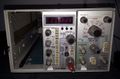
DC503 early operating.jpg | DC503 front (older version) in operation | |||
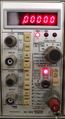
Tek | Tek dc503 fronttop.jpg | DC503 front (older version) | ||
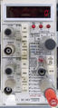
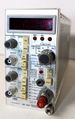
Tek | Tek-dc503-front.jpg | DC503 front (newer version) | ||
</gallery> | Tek dc503 on.jpg | DC503 in operation | ||
Tek dc503.jpg | |||
Tek dc503 pg502.jpg | DC503 and [[PG502]] in a [[TM503]] | |||
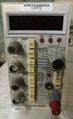
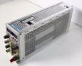
Tek dc503 rear.jpg | DC503 rear | |||
Tek dc503 top.jpg | DC503 top | |||
Tek dc503 34.jpg | |||
</gallery> | |||
==Components== | ==Components== | ||
{{Parts|DC503}} | {{Parts|DC503}} | ||
Latest revision as of 06:02, 6 October 2024

The Tektronix DC503 is a 100 MHz, 7-digit frequency counter plug-in for the TM500 system. . It was introduced in 1972 at the launch of the TM500 system, and superseded by the DC503A in 1981.
Opt.01 is an OCXO for improved stability.
Key Specifications
| Resolution | 7 digits |
|---|---|
| Frequency Range | 0.1 Hz (AC coupled: 10 Hz) to 100 MHz |
| Impedance | 1 MΩ paralleled by approx. 20 pF |
| Sensitivity | 300 mVp-p sinewave times attenuation to 100 MHz |
| Max Input Voltage, 1× Att. | 50 V @ ≤2 kHz, derate –20 dB/decade to 10 MHz; 10 V @ 10 kHz to 25 MHz, derate –20 dB/decade to 50 MHz; 5 V @ 50 MHz to 100 MHz |
| Max Input Voltage, 10×/100× Att. | 500 V @ ≤2 MHz, derate –20 dB/decade to 100 MHz |
| — Standard time base — | |
| Frequency | 1 MHz ± 1 × 10⁻⁷ at cal |
| Error | ≤ ±1 × 10⁻⁵ from 0 °C to +50 °C |
| Aging | ≤ ±1 × 10⁻⁵ per month |
| — Opt.01 OCXO time base — | |
| Frequency | 5 MHz ± 5 × 10⁻⁹ at cal |
| Error | ≤ ±5 × 10⁻⁷ from 0 °C to +50 °C (after oven warm-up) |
| Aging | ≤ ±1 × 10⁻⁷ per month |
Gerbers
Rear interface
| 27A – Internal scan clock disable | |
| 26A − Reset, in/out | |
| 25B − Ext scan clock in | 25A − Time slot zero (TS0) |
| 24B − Scan clock out | |
| 23B − Overflow disp.dis. in | |
| 22B − Overflow out | |
| 21B − BCD out 2 | 21A − TTL Clock Input |
| 20B − BCD out 8 | 20A − BCD out 4 |
| 19B − Latch Out (Data Good) | 19A − BCD out 1 |
| 17B – Ch B Input | 17A – Ch A Input GND |
| 16B – Ch B Input GND | 16A − Ch A Input |
| 14A − 1 MHz clock out |
Links
Documents Referencing DC503
Patents that may apply to DC503
| Page | Title | Inventors | Filing date | Grant date | Links |
|---|---|---|---|---|---|
| Patent US 3562464A | Cam actuated switch having movable and fixed contacts on circuit board | Howard Vollum • Willem H Verhoef • Tony Sprando | 1968-10-07 | 1971-02-09 | Cam switches • 1501 • 2101 • 2701 • 2703 • 432 • 434 • 465 • 475 • 5A15N • 5A18N • 5A20N • 5A21N • 5A38 • 5A45 • 5B10N • 5B12N • 7A15 • 7A16A • 7A18 • 7A19 • 7A24 • 7A26 • 7B10 • 7B15 • 7B50 • 7B51 • 7B52 • 7B53A • 7B50A • 7B70 • 7B71 • 7B80 • 7B85 • 7B87 • 7B92 • 7B92A • 7D01 • 7D12 • 7D15 • 7J20 • 7S12 • 7T11 • 7T11A • AF501 • AM502 • AM503 • DC502 • DC503 • DC504 • DC505 • DM501 • DM502 • FG501 • FG501A • FG502 • FG503 • FG504 • FG507 • PG501 • PG502 • PG505 • PG506 • PG506A • PG508 • TG501 • SC502 • SC503 • SC504 |
Pictures
-
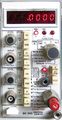
DC503 front (older version) in operation
-
DC503 front (older version)
-

DC503 front (newer version)
-
DC503 in operation
-
-
-

DC503 rear
-
DC503 top
-


Components
Some Parts Used in the DC503
| Part | Part Number(s) | Class | Description | Used in |
|---|---|---|---|---|
| 2N4249 | 151-0342-00 | Discrete component | Si PNP low-noise transistor | DC501 • DC502 • DC503 • DC503A • DC504 • DC504A • DC505 • DC505A • DC508 • DC508A • DC509 • DC510 |
| 2N4851 | 151-0504-00 • 151-0504-01 | Discrete component | silicon unijunction transistor | DC501 • DC502 • DC503 • DC503A • DC504 • DC505 • DC505A • DC508 • DC508A • LA501 • R1330 • 212 • 214 • 4002A • 4623 • 4631 • 4632 • 4633A • 4634 • 4701 • 4701R • 670-0696-01 • 670-1274-00 • 670-1981-00 • 670-1981-01 • 7D01 • 7D12 • 7L12 |